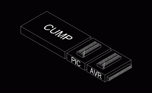
Communitary Universal Microcontroller Programmer

Status
This project is being actively developed. Visit the
CUMP mailing list for more
information.
History / Beginning
An open source project:
It all started with a post on the PICList you can
read the original PICList threads starting here:
Edson Brusque
started the CUMP mailing list
on http://groups.yahoo.com.
Resolutions
All parts easily obtained and assembled at low cost by beginners.
Abstracted interface (modular, can be serial, parallel, USB, etc...) and
using a command language that will be easy to send from any host including an
ASCII dumb terminal.
High level language text or tokens sent to MB processor which is either
- compiled into tokens (if not already compiled on the host) and stored
either
- in the MB processor (RAM or EEPROM) for later direct execution or
- in an optional serial EEPROM on the DB for later retrieval and execution
without need for download of anything other than programming data from the
host. Each DB can know how to program a different device allowing for
production programming.
- interpreted into programming data and programmed into the target using
token code from the DB or MB. Intel Hex format 8M is the default but others
will follow.
- directly executed to allow for immediate
- status read-back, (installed options/modules/target device, data needed to
program installed device, menu)
- action initiation, or
- other general purpose computing (use of the CUMP as a logic analyzer,
controller, programmable powersupply, meter, etc...with low-level functions to
generate sine, triangle, saw and pulse waves outputs and to read pins inputs
and A/Ds)
A 40 pin connector interface to a matching socket on the DB (Daughter Board:
Where the programming socket and any additional circuitry necessary for the
device being programmed reside) so that direct plug in, ribbon cable, card slot
connector, DIL pins to cable, etc... can be used. The pin assignements have
been set:
  1 SCK_SCL (SPI & I2C clock)
  2 GND
  3 SDI_SDA (SPI & I2C data)
  4 SDO (SPI data)
  5 TxD (UART Transmit)
  6 +5V
  7 RxD (UART Receive)
  8 BD0 (Bi-Directional 0)
  ...
35 BD27 (Bi-Directional 27)
36 VAR1 (Variable Voltage Supply 1)
37 VAR2 (Variable Voltage Supply 2)
38 BD28 (optional)
39 BD29 (optional)
40 BD30 (optional)
Space available on MB for extra latches, with software support but these are
not required and can be left off for targets that are serially programmed or
they can be moved to a DB.
Multiple Variable high voltage
supplys on the motherboard or manually adjustable
depending on how the builder wants to do it.
See also
Summary
A universal programmer that operates independant of operating system, can
program any device via "daughter boards"(DBs) which are adaptor
boards that will plug into the main board. The Main Board (MB) will have
various circuits designed to provide compatability with almost any device.
There will be a power supply board that is seperate, due to the large amount of
argument surrounding that subject. There will also be a one time programming
board to get the firmware onto the MCU on the MB. And, there will be a board
for communication interfacing so that the programmer will not be resricted to
any specific protocol.
Firmware:
- Consists of control algorithms for all of the built-in devices, and a
byte code interpreter for allowing easy writing of
programming algorithms.
Hardware:
- MB
- The Main Board will have:
- A PIC16F877 to handle control
- An 8-pin ICSP compatible header
- A 40-pin or 37-pin header to connect to DB's
- A 10-pin header to connect to the Power supply
- An 10-pin communication header
- An optional I2C hub
- Optional I2C expansion ports
- An optional onboard MAX232 for onboard RS232 communication
- Additional required components for the operation of the MCU
- Several DIP switches for signal switching and configuration
(Note: the choice of controller is currently under "discussion" on
the CUMP list. I have posted a comparison table of available MCUs that could
fit the bill.)
- A ZIF socket physically mounted to the main unit or to a daughter board
with a large pin header where each pin of the ZIF can be connected to any pin
of the DB Header. This will allow the programming of most devices with just a
low cost female header to connect the signals to the correct target pins for
each type of device.
- DB
- The DBs will have:
- An optional (Recomended) onboard EEPROM to store the bytecode instructions
for the MB processor.
- A 40-pin/37-pin header for connection to the MB and supply voltages.
- All additional required hardware for the target device.
- Comm Board
- The Comm Board will have:
- All required communications hardware for conversion from SPI, I2C or
USART serial to the target protocol
- A 10-pin header encompasing all the previously mentioned protocols
- PSupply
- The supply board wil have:
- The required hardware for a 25V source
- The required hardware for a 5V source
- The required hardware for 2 programable sources and any of the following
desired to make said sources
- 2 PWM inputs for voltage control (optional)
- 2 analog feedback returns (optional)
- An I2C port (optional)
- 2 buffered full scale analog outputs
Previous recommendations considered by the list
Hardware
It has been suggested that the SIMM form factor be adopted.
(Note: The SIMM form factor has been essentially rejected due to various
reasons. Visit the CUMP mailing list archives for more info) This would make
the product compatible with the
A ZIF socket not permanently connected to any one DB, with a 40-pin header
so that it can be connected to a second 40-pin header on any DB.
A device similar to a breakout box for extremely cheap (but slow) rerouting
of traces for programming, but that should be a DB.
Software
Byron A Jeff has
recommended the use of the IPL license from
http://www.sci.usq.edu.au/staff/house/ipl/ipl.htm(Note:
He has recently said that the GPL would likely be more appropriate for this
project)
Suggestions
See also:

