SX User’s Manual Rev. 3.1
21
© 2000 Scenix Semiconductor, Inc. All rights reserved.
www.scenix.com
Chapter 2
Architecture
2.1 Introduction
The SX device is a complete RISC communications controller with an electrically erasable (flash)
program memory and in-system programming capability. The device can operate with a clock rate of
up to 75 MHz and can execute instructions at a rate of up to 75 million instructions per second.
The SX device has multi-pin I/O ports, an internal oscillator, a Watchdog timer, a Real-Time Clock/
Counter, an analog comparator, power-on and brownout reset control, and Multi-Input Wakeup
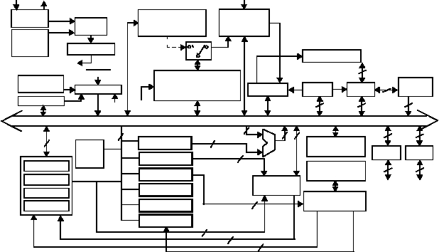
capability. Figure 2-1 is a block diagram showing the core features of the basic device. Additional
features are available with some SX family members. For example, some devices offer more RAM, a
larger EEPROM program memory, or additional peripheral modules such as multi-function timers.
Figure 2-1 SX28AC Block Diagram
Interrupt
M IW U
Port B
Com p
Power-On
Reset
RESET
8-bit W atchdog
Timer (W DT)
8-bit Timer
RTCC
8
8
8
Port C
8
8
Port A
8
4
Internal Data Bus
In-System
Debugging
In-System
Program m ing
2k W ords
EEPRO M
System
Clock
Brown-O ut
M IW U
M CLR
O SC
Driver
4MHz
Internal
RC O SC
Clock
Select
¸ 4 or ¸ 1
136 Bytes
SRAM
Address
W rite Data
Read Data
Instruction
W
FSR
STATUS
PC
M ODE
OPTIO N
System Clock
O SC1 OSC2
Fetch
8
8
12
Address
12
8
8
8
8
ALU
8
8
8
3
RTCC
Analog
8
Interrupt Stack
PC
3 Level
Decode
Executive
W rite Back
IREAD
Stack
Instruction
Pipeline
Prescaler for RTCC
or
Prescaler for W DT
