SX User’s Manual Rev. 3.1
150
© 2000 Scenix Semiconductor, Inc. All rights reserved.
www.scenix.com
Chapter 5 Input/Output Ports
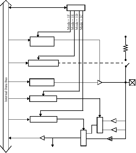
The block diagram in Figure 5-1 is for a Port B data pin, but the same diagram also applies to pins of
the other ports, with one exception. Port A does not offer a Schmitt trigger input option, so it lacks the
control register bit and logic associated with the Schmitt trigger buffer.
Figure 5-1 Port B Pin Block Diagram
MODE
RB
PL P_B
LVL_B
0 = Output
1 = Hi-Z Input
0 = Pullup Enable
1 = Pullup Disable
RD*/WR
0 = CMOS
1 = TTL
RD
Port B: Input, MIWU, Comparator
VDD
Pullup Resistor
(~20kW)
Port B
M
U
X
ST_B
RD*/WR
0 = Schmitt Trigger Enable
1 = Schmitt Trigger Disable
TTL Buffer
CMOS Buffer
M
U
X
Schmitt Trigger Buffer
Direction
RB Data
RD*/WR
R D*/W R
RD*/WR
* RD (Read) on SX48BD/52BD only
