SX User’s Manual Rev. 3.1
138
© 2000 Scenix Semiconductor, Inc. All rights reserved.
www.scenix.com
Chapter 4 Clocking, Power Down, and Reset
4.5 Reset
A reset operation puts the SX device into a known initial state. A reset occurs upon any one of the
following conditions:
•
initial power-up
•
wakeup from the power down mode
•
recovery from brown-out, as determined by the brown-out detection circuit
•
Watchdog timeout
•
assertion of the MCLR input signal (Master Clear Reset)
When a reset occurs, the program counter is initialized to the highest program address (7FFh or FFFh,
depending on the SX device type), where the application program should have a “jump” instruction to
its initialization routine.
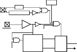
Figure 4-5 shows the internal logic of the SX reset circuit. This circuit senses the voltage supply on the
VDD pin, the state of the MCLR (Master Clear Reset) input pin, the output of the on-chip RC oscillator,
and signals from the Multi-Input Wakeup circuit and Watchdog timer. Based on these inputs, the
circuit generates a chip-internal RESET signal. This signal goes low to put the device into the reset
state and then goes high to allow the device to begin operating from a known state.
4.5.1
Register States Upon Different Resets
The effect of different reset operations on a register depends on the register and the type of reset
operation. Some registers are initialized to specific values, some are left unchanged (for wakeup and
brown-out resets), and some are initialized to an unknown value. A register that starts with an unknown
value should be initialized by the software to a known value; you cannot simply test the initial state
and rely on it starting in that state consistently.
Figure 4-5 On-Chip Reset Circuit Block Diagram
POR
BROWN-OUT
MIWU
MCLR/Vpp pin
wdt_time_out
10-Bit Asynch
Ripple
Counter
(Start-Up
Timer)
VDD
rc_clk
drt_time
_out
S
R
Q
QN
RESET
POR
