© 2005 Ubicom, Inc. All rights reserved.
- 27 -
www.ubicom.com
SX20AC/SX28AC
12.0 RESET
Power-On-Reset, Brown-Out reset, watchdog reset, or
external reset initializes the device. Each one of these
reset conditions causes the program counter to branch to
the top of the program memory. For example, on the
device configured for 2048 words of program memory,
the program counter is initialized to 07FF.
The device incorporates an on-chip Power-On Reset
(POR) circuit that generates an internal reset as V
dd
rises
circuit. The circuit contains an 10-bit Delay Reset Timer
(DRT) and a reset latch. The DRT controls the reset time-
out delay. The reset latch controls the internal reset sig-
nal. Upon power-up, the reset latch is set (device held in
reset), and the DRT starts counting once it detects a valid
logic high signal at the MCLR pin. Once DRT reaches the
end of the timeout period (typically 72 msec), the reset
latch is cleared, releasing the device from reset state.
If the device has already been released from the 72ms
power-on-reset delay, and an MCLR pin reset is
asserted, the device typically takes only 20ms to leave
the reset state, after the rising edge of MCLR.
not tied to the V
dd
pin and V
dd
signal is allowed to rise
and stabilize before MCLR pin is brought high. The
device will actually come out of reset T
drt
msec after
MCLR goes high.
The brown-out circuitry resets the chip when device
power (V
dd
) dips below its minimum allowed value, but
not to zero, and then recovers to the normal value.
.
Note:Ripple counter is 10 bits for Power on Reset (POR)
only.
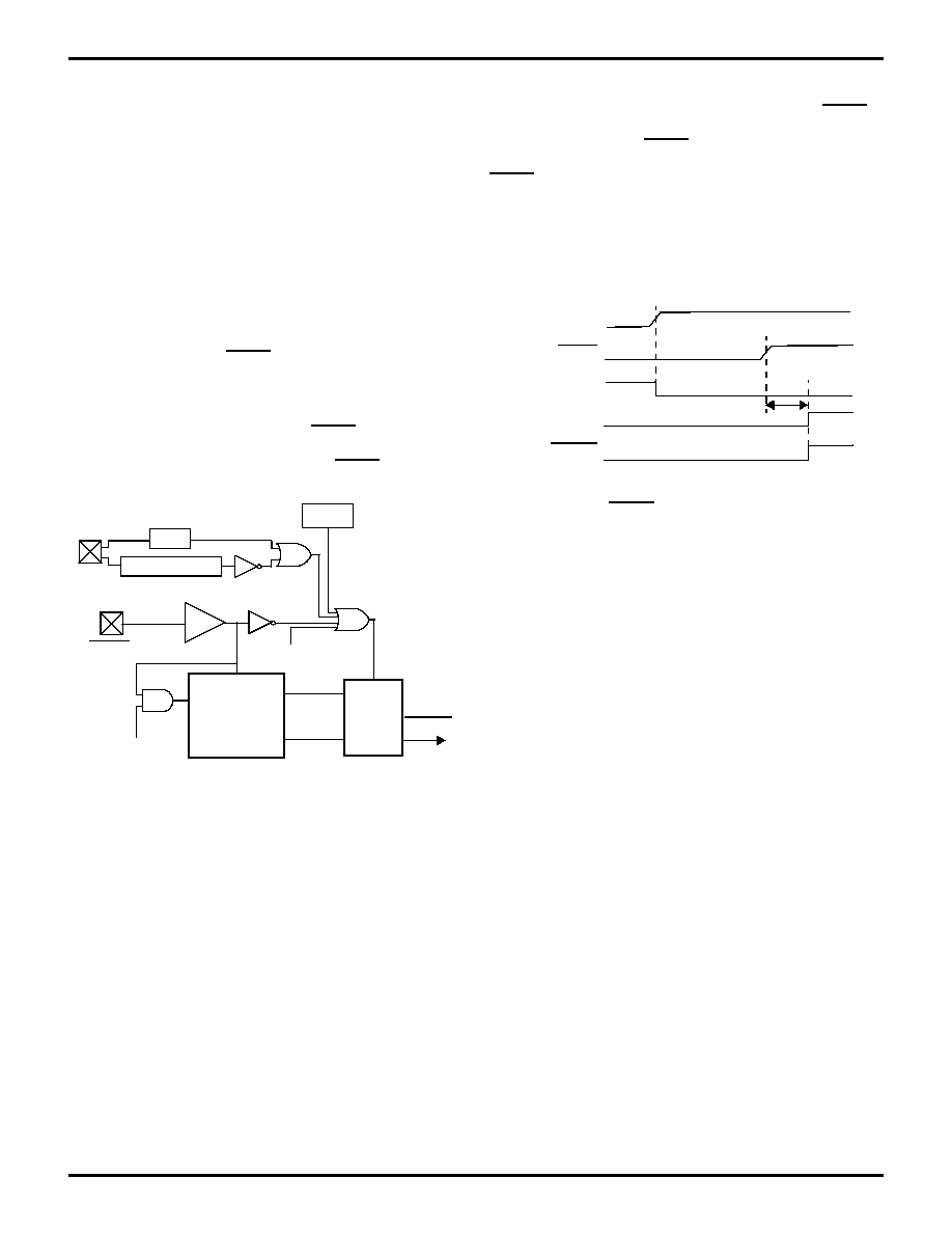
Figure 12-1. Block Diagram of On-Chip Reset Circuit
POR
BROWN-OUT
MIWU
MCLR/Vpp pin
wdt_time_out
10-Bit Asynch
Ripple
Counter
(DRT Start-Up
Timer)
V
dd
rc_clk
drt_time
_out
S
R
Q
QN
RESET
POR
enable
Figure 12-2. Time-Out Sequence on Power-Up
(MCLR not tied to V
dd
)
V
dd
MCLR
POR
drt_time_out
RESET
Tdrt

