© 2005 Ubicom, Inc. All rights reserved.
- 17 -
www.ubicom.com
SX20AC/SX28AC
7.0 POWER DOWN MODE
The power down mode is entered by executing the
SLEEP instruction. Execution of the SLEEP instruction
causes the clock to the device to be stopped.
In power down mode, only the Watchdog Timer (WDT) is
active. If the Watchdog Timer is enabled, upon execution
of the SLEEP instruction, the Watchdog Timer is cleared,
the TO (time out) bit is set in the STATUS register, and
the PD (power down) bit is cleared in the STATUS regis-
ter.
There are three different ways to exit from the power
down mode: a timer overflow signal from the Watchdog
Timer (WDT), a valid transition on any of the Multi-Input
Wakeup pins (Port B pins), or through an external reset
input on the MCLR pin.
To achieve the lowest possible power consumption, the
Watchdog Timer should be disabled and the device
should exit the power down mode through the Multi-Input
Wakeup (MIWU) pins or an external reset.
7.1 Multi-Input Wakeup
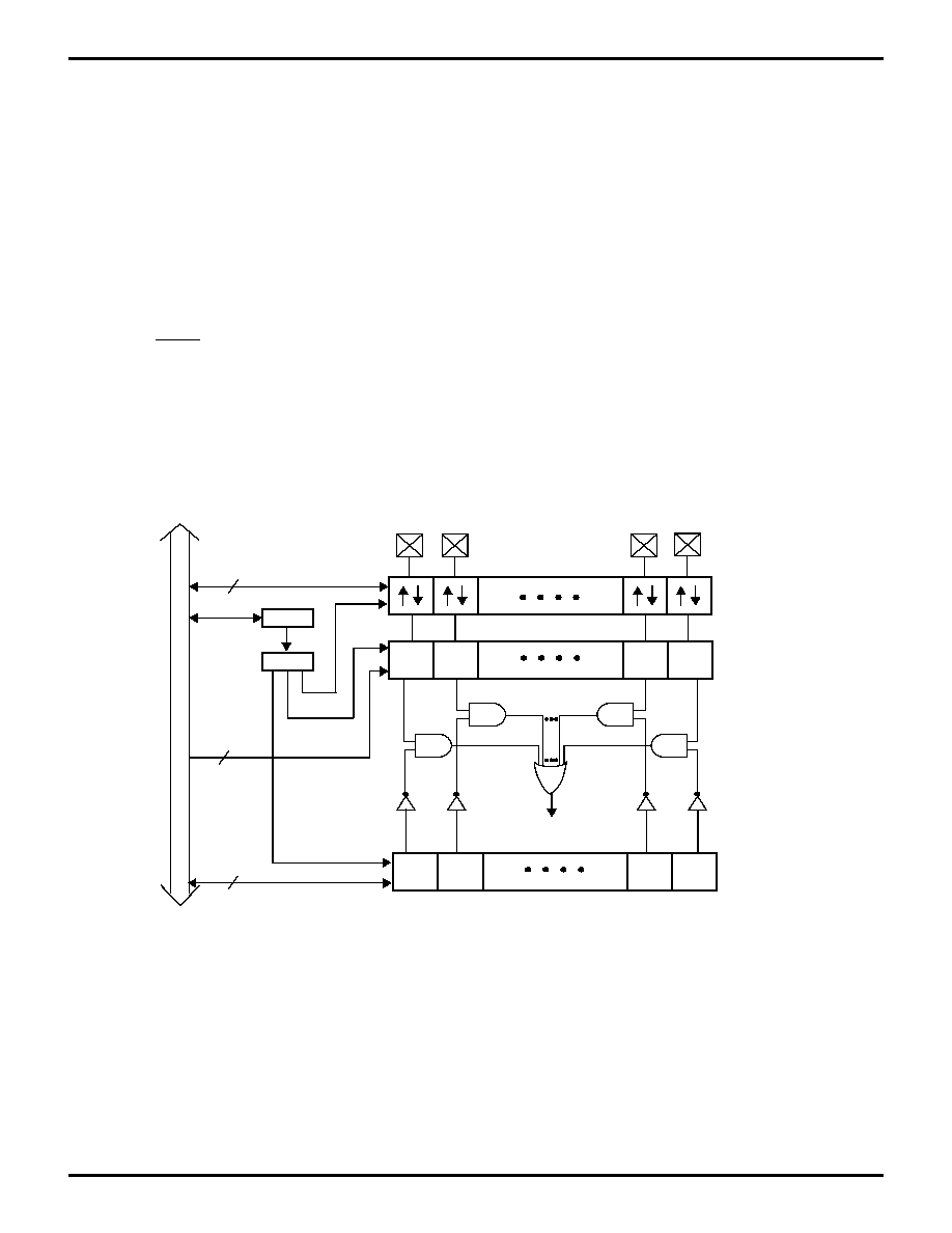
Multi-Input Wakeup is one way of causing the device to
exit the power down mode. Port B is used to support this
feature. The WKEN_B register (Wakeup Enable Regis-
ter) allows any Port B pin or combination of pins to cause
the wakeup. Clearing a bit in the WKEN_B register
enables the wakeup on the corresponding Port B pin. If
multi-input wakeup is selected to cause a wakeup, the
trigger condition on the selected pin can be either rising
edge (low to high) or falling edge (high to low). The
WKED_B register (Wakeup Edge Select) selects the
desired transition edge. Setting a bit in the WKED_B reg-
ister selects the falling edge on the corresponding Port B.
Clearing the bit selects the rising edge. The WKEN_B
and WKED_B registers are set to FFh upon reset.
Once a valid transition occurs on the selected pin, the
WKPND_B register (Wakeup Pending Register) latches
the transition in the corresponding bit position. A logic `1'
indicates the occurrence of the selected trigger edge on
the corresponding Port B pin.
Upon exiting the power down mode, the Multi-Input
Wakeup logic causes program counter to branch to the
maximum program memory address (same as reset).
Figure 7-1 shows the Multi-Input Wakeup block diagram.
Figure 7-1. Multi-Input Wakeup Block Diagram
W
Internal Dat
a
Bus
MODE
Wake-up: Exit Power Down
8
8
RB7
RB6
RB1 RB0
WKED_B
WKPND_B
WKEN_B
MODE = 09
MODE = 0B
MODE = 0A
Port B
Configured
as Input
0 1
8
0 = Enable
1 = Disable
