From Saurabh Gupta and Dhananjay V Gadre, Netaji Subhas Institute of Technology, Dwarka, New Delhi, India
This method allows 2×N×(N–1) LEDs using only N I/O lines and a few additional discrete components. The technique exploits the fact that each I/O line has three states: one, zero, and high impedance. Thus, with two I/O lines, states 00, 01, 10, and 11 of eight possible states control the LEDs.
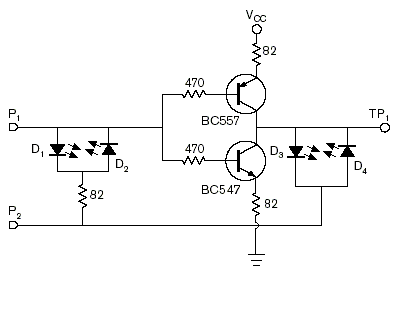
Here is an example with two I/O lines controlling four LEDs. P1 and P2 are the inputs. The circuit requires that the LED turn-on voltage should be slightly more than VCC/2. For red LEDs with a turn-on voltage of approximately 1.8V, a suitable supply voltage is 2.4V. For blue or white LEDs, you can use a 5V supply voltage. For N I/O lines, this technique requires N–1 transistor pairs.
Here are the states of P1 and P2 as they relate to which LED lights up:
| P1 | P2 | TP1 | LED |
| 0 | 0 | Vcc | D3 |
| 0 | 1 | Vcc | D2 |
| 1 | 0 | 0 | D1 |
| 1 | 1 | 0 | D4 |
| Z | Z | Vcc/2 | None |
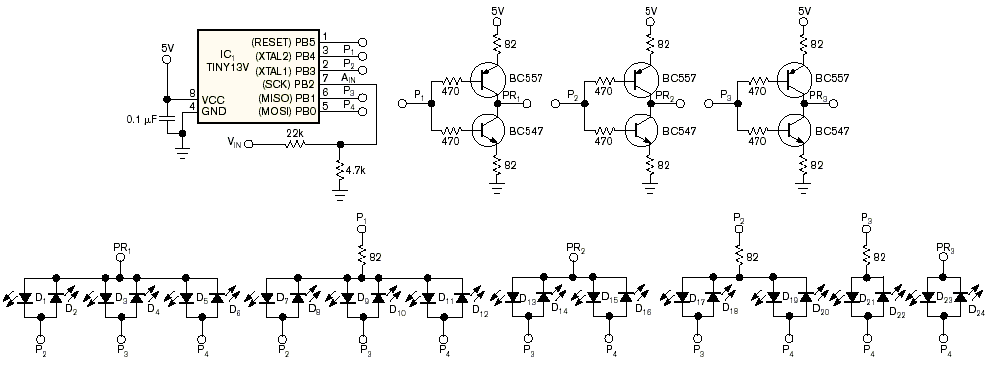
A second example shows 24 white LEDs with 4 IO pins and 6 transistors controlled by an ATMEL AT Tiny 13 Microcontroller.
And here is the C source code for a bargraph display with the analog input comming into PB2 (pin 7, Ain).
/*Saurabh Gupta and Dhananjay V. Gadre*/
/*Tiny13 Processor*/

/* January 2008*/

#include<avr/io.h>
#include<avr/interrupt.h>
#include<avr/pgmspace.h>

typedef unsigned char u08;

void delay(u08 a)
{

u08 i,j;

	for(i=0;i<a;i++)
	{
		for(j=0;j<250;j++)
		{
			asm("nop");
			asm("nop");
			asm("nop");
			asm("nop");
		}
	}
}


const unsigned char portb_value[] PROGMEM = {
	0b00000000
,	0b00011000
,	0b00000000
,	0b00010010
,	0b00000000
,	0b00010001
,	0b00010000
,	0b00001000
,	0b00010000
,	0b00000010
,	0b00010000
,	0b00000001
,	0b00000000
,	0b00001010
,	0b00000000
,	0b00001001
,	0b00001000
,	0b00000010
,	0b00001000
,	0b00000001
,	0b00000010
,	0b00000001
,	0b00000000
,	0b00000011
	};

//port_value[0]-->for L0		(1st led)
//port_value[23]-->for L23		(24th led)

const u08 ddrb_value[] PROGMEM = {
	0b00011000
,	0b00011000
,	0b00010010
,	0b00010010
,	0b00010001
,	0b00010001
,	0b00011000
,	0b00011000
,	0b00010010
,	0b00010010
,	0b00010001
,	0b00010001
,	0b00001010
,	0b00001010
,	0b00001001
,	0b00001001
,	0b00001010
,	0b00001010
,	0b00001001
,	0b00001001
,	0b00000011
,	0b00000011
,	0b00000011
,	0b00000011
	};


u08 value=0,count=0;


ISR(TIM0_OVF_vect)				//1200 Hz
{
//delay(100);
	TCNT0=-32;
	ADCSRA|=(1<<ADSC);
//	if(value!=0)
	count=(count<value)?(count+1):0;

//	else
//	count=0;

//count=(count<24)?count:0;

	DDRB=pgm_read_byte(ddrb_value + count);
	PORTB=pgm_read_byte(portb_value + count);

}


ISR(ADC_vect)
{

int temp;
u08 temp2;

temp2=ADCH;


temp=temp2*15;
temp=temp>>7;

value=temp;

value=(value<24)?value:24;


}


int main()
{

	DDRB=0x00;
	PORTB=0x00;

TCCR0A=0X00;
//    TCCR0A - Timer/Counter Control Register A
//    ---------------------------------------------------------
//    |COM0A1|COM0A0|COM0B1|COM0B0|  –   |  –   | WGM01| WGM00|
//    |  7   |  6   |  5   |  4   |  3   |  2   |  1   |  0   |
//    ---------------------------------------------------------

TCCR0B=(1<<CS02);		//9.6 MHz divided by 256
//    TCCR0B - Timer/Counter Control Register B
//    -------------------------------------------------
//    |FOC0A|FOC0B|  –  |  –  |WGM02| CS02| CS01| CS00|
//    |  7  |  6  |  5  |  4  |  3  |  2  |  1  |  0  |
//    -------------------------------------------------


TIMSK0=(1<<TOIE0);
//    TIMSK - Timer/Counter Interrupt Mask Register
//    ---------------------------------------------------------
//    |  -   |	-	|  -   |  -	  |OCIE0A|OCIE0B|TOIE0 |  -   |
//    |  7   |  6   |  5   |  4   |  3   |  2   |  1   |  0   |
//    ---------------------------------------------------------

TCNT0=-32;		//1200 Hz


	ADMUX=(1<<REFS0)|(1<<ADLAR)|(1<<MUX0);
//    ADMUX - ADC Multiplexer Selection Register
//    -------------------------------------------------
//    |	 -	|REFS0|ADLAR|  -  |  -  |  -  | MUX1| MUX0|
//    |  7  |  6  |  5  |  4  |  3  |  2  |  1  |  0  |
//    -------------------------------------------------

	ADCSRA=(1<<ADEN)|(1<<ADIE)|(1<<ADPS2);
//    ADCSRA - ADC Control and Status Register A
//    -------------------------------------------------
//    |ADEN |ADSC |ADATE| ADIF| ADIE|ADPS2|ADPS1|ADPS0|
//    |  7  |  6  |  5  |  4  |  3  |  2  |  1  |  0  |
//    -------------------------------------------------

	ADCSRB=0x00;

	DIDR0 = (1<<ADC1D);	//Disable Digital input buffer on PB5
//    DIDR0 - Digital Input Disable Register 0
//    -------------------------------------------------
//    |  –  |  –  |ADC0D|ADC2D|ADC3D|ADC1D|AIN1D|AIN0D|
//    |  7  |  6  |  5  |  4  |  3  |  2  |  1  |  0  |
//    -------------------------------------------------

sei();

while(1);

return 0;

}