DC biasing is setting up a circuit to operate a transistor at a desired operating point on its characteristic curve. Three bias networks for the common emitter amplifier are shown in figure 5.7.
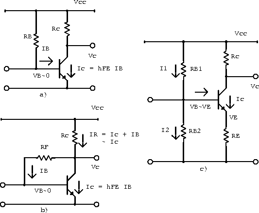
Figure 5.7: Bias circuits for the common emitter
amplifier.
In figure 5.7a the only path for DC bias current into the
base is through ![]() .
.
![]() is a power supply voltage which is generally greater than
10 V such that
is a power supply voltage which is generally greater than
10 V such that ![]() can be ignored.
The DC voltage at the collector should be large enough to provide at
least a 2 V drop between collector and emitter and clearly must be
less than
can be ignored.
The DC voltage at the collector should be large enough to provide at
least a 2 V drop between collector and emitter and clearly must be
less than ![]() .
In the absence of other circuit requirements, a convenient algebraic
choice for
.
In the absence of other circuit requirements, a convenient algebraic
choice for ![]() is
is ![]() .
DC circuit analysis results in the following relative sizes of the two
resistors:
.
DC circuit analysis results in the following relative sizes of the two
resistors:
![]()
Although the circuit works reasonably well, the fact that ![]() is
quite variable among samples leads to a bad design.
A well-designed circuit should have an operating point that is less
dependent on this parameter.
is
quite variable among samples leads to a bad design.
A well-designed circuit should have an operating point that is less
dependent on this parameter.
Figure 5.7b shows a network with the base-biasing resistor
connected to the collector instead of ![]() .
.
![]() acts as a negative feedback resistor since it feeds the
collector current back into the base.
Analysis gives
acts as a negative feedback resistor since it feeds the
collector current back into the base.
Analysis gives
![]()
Therefore a change in ![]() has only half the effect of the
previous design.
has only half the effect of the
previous design.
A more common bias stabilization technique employs a series resistor
between the emitter and ground.
This circuit has about the same sensitivity to changes in ![]() as
the previous circuit.
as
the previous circuit.
A further improvement can be made by introducing a second base-bias resistor as shown in figure 5.7c. The bias voltage is determined almost entirely by the two bias resistors. These biasing methods can also be used for the common collector and common base configurations.