SX User’s Manual Rev. 3.1
165
© 2000 Scenix Semiconductor, Inc. All rights reserved.
www.scenix.com
Chapter 8
Multi-Function Timers
8.1 Introduction
Some SX devices such as the SX48/52BD have a set of on-chip multi-function timers in addition to
the standard RTCC and Watchdog timers found in all SX devices. The SX48/52BD has two such
multi-function timers, designated T1 and T2. These versatile, programmable timers reduce the
software burden on the CPU in real-time control applications such as PWM generation, motor control,
triac control, variable-brightness display control, sine wave generation, and data acquisition.
Each timer consists of a 16-bit counter register supported by a 16-bit capture register and a 16-bit
comparison register. Each timer uses up to four I/O pins: one clocking input, two capture inputs, and
one timer output. The timer I/O pins are alternate functions of Port B pins for timer T1 and Port C pins
for Timer T2.
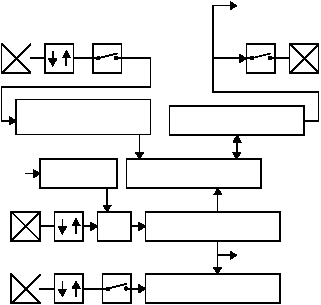
Figure 8-1 is a block diagram showing the registers and I/O pins of one timer. The 16-bit free-running
timer/counter register is initialized to 0000h upon reset and counts upward continuously. It is clocked
either by an external signal provided on an I/O pin or by the on-chip system clock divided by a value
selected by a 3-bit divide-by factor.
Figure 8-1 Multi-Function Timer Block Diagram
Ext. Clock
Capture 1
Capture 2
3-bit Divide-by
16-Bit Free-Running
16-Bit Comparator
16-Bit Comparison Register R1
Timer/Counter
16-Bit Capture Register (1)
MUX
match
Output
Compare Interrupt
System
Clock
Capture Interrupt
16-Bit Comparison Register R2
or
16-Bit Capture Register (2)
Factor
