© 2000 Scenix Semiconductor, Inc. All rights reserved.
7
SX Device Programming Specifications Rev 2.2
www.scenix.com
2.4 Internal Hardware
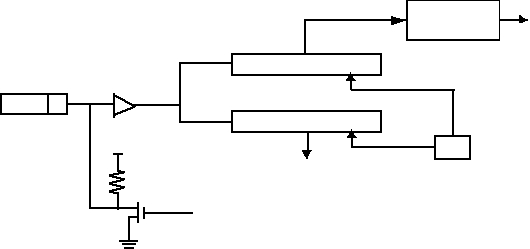
Figure 2.4 is a simplified block diagram of the chip-internal ISP hardware.
Serial data written to the OSC2 pin is shifted into the command shift register or data shift register,
depending on whether command bits or data bits are being processed within a frame. Command bits
are decoded and used to control the flash EEPROM block, while data bits are written to the flash
EEPROM.
When the command is to read data from the program memory, the data bits are read from the EEPROM
block and shifted out on the OSC2 pin during the data cycles. An open-drain transistor and a pullup
resistor pull the OSC2 pin low or high for each bit. This same transistor is used to pull the OSC2 pin
low during the second clock within each cycle (except in the sync cycle).
Figure 2.4 ISP Circuit Block Diagram
OSC2
COMMAND SHIFT REG
To EEPROM IN
clk
serial data out
(from EEPROM)
EEPROM
CONTROL
COMMAND
DATA SHIFT REG
DECODE
