© 2000 Scenix Semiconductor, Inc. All rights reserved.
- 41 -
www.scenix.com
SX48BD/SX52BD/SX52BD75/SX52BD100
15.0
INSTRUCTION SET
As mentioned earlier, the SX family of devices uses a
modified Harvard architecture with memory-mapped
input/output. The device also has a RISC type architec-
ture in that there are 43 single-word basic instructions.
The instruction set contains byte-oriented file register, bit-
oriented file register, and literal/control instructions.
Working register W is one of the CPU registers, which
serves as a pseudo accumulator. It is a pseudo accumu-
lator in a sense that it holds the second operand,
receives the literal in the immediate type instructions, and
also can be program-selected as the destination register.
The bank of 31 file registers can also serve as the pri-
mary accumulators, but they represent the first operand
and may be program-selected as the destination regis-
ters.
15.1
Instruction Set Features
1. All single-word (12-bit) instructions for compact code
efficiency.
2. All instructions are single cycle except the jump type in-
structions (JMP, CALL) and failed test instructions
(DECSZ fr, INCSZ fr, SB bit, SNB bit), which are two-
cycle.
3. A set of file registers can be addressed directly or indi-
rectly, and serve as accumulators to provide first oper-
and; W register provides the second operand.
4. Many instructions include a destination bit which se-
lects either the register file or the accumulator as the
destination for the result.
5. Bit manipulation instructions (Set, Clear, Test and Skip
if Set, Test and Skip if Clear).
6. STATUS Word register memory-mapped as a register
file, allowing testing of status bits (carry, digit carry, ze-
ro, power down, and timeout).
7. Program Counter (PC) memory-mapped as register file
allows W to be used as offset register for indirect ad-
dressing of program memory.
8. Indirect addressing data pointer FSR (file select regis-
ter) memory-mapped as a register file.
9. IREAD instruction allows reading the instruction from
the program memory addressed by W and upper four
bits of MODE register.
10.Eight-level, 12-bit push/pop hardware stack for sub-
routine linkage using the Call and Return instructions.
11.Seven addressing mode provide great flexibility.
15.2
Instruction Execution
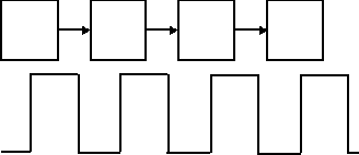
An instruction goes through a four-stage pipeline to be
executed (Figure15-1). The first instruction is fetched
from the program memory on the first clock cycle. On the
second clock cycle, the first instruction is decoded and
the second instruction is fetched. On the third clock cycle,
the first instruction is executed, the second instruction is
decoded, and the third instruction is fetched. On the
fourth clock cycle, the first instruction’s results are written
to its destination, the second instruction is executed, the
third instruction is decoded, and the fourth instruction is
fetched. Once the pipeline is full, instructions are exe-
cuted at the rate of one per clock cycle.
Instructions that directly affect the contents of the pro-
gram counter (such as jumps and calls) require that the
pipeline be cleared and subsequently refilled. Therefore,
these instructions take more than one clock cycle.
The instruction execution time is derived by dividing the
oscillator frequency by one (bit 11 of the FUSE Word reg-
ister must be initialized to 0).
Figure 15-1. Pipeline and Clock Scheme
Fetch
Decode
Execute
Write
Clock
Cycle
1
Clock
Cycle
2
Clock
Cycle
3
Clock
Cycle
4
