© 2000 Scenix Semiconductor, Inc. All rights reserved.
- 38 -
www.scenix.com
SX48BD/SX52BD/SX52BD75/SX52BD100
12.0
RESET
Power-On-Reset, Brown-Out reset, watchdog reset,
wakeup reset, or external reset initializes the device.
Each one of these reset conditions causes the program
counter to branch to the top of the program memory
(FFFh).
The device incorporates an on-chip Power-On Reset
(POR) circuit that generates an internal reset as Vdd rises
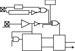
during power-up. Figure 12-1 shows the block diagram of
the circuit. The circuit contains a 10-bit Delay Reset
Timer (DRT) (2 bits contained in the FUSEX register) and
a reset latch. The DRT controls the reset timeout delay.
The reset latch controls the internal reset signal. Upon
power-up, the reset latch is set (device held in reset), and
the DRT starts counting once it detects a valid logic high
signal at the MCLR pin. Once DRT reaches the end of
the timeout period (default of 18 msec), the reset latch is
cleared, releasing the device from reset state.
Figure 12-2 shows a power-up sequence where MCLR is
not tied to the Vdd pin and Vdd signal is allowed to rise
and stabilize before MCLR pin is brought high. The
device will actually come out of reset Tdrt msec after
MCLR goes high.
The brown-out circuitry resets the chip when device
power (Vdd) dips below its minimum allowed value, but
not to zero, and then recovers to the normal value.
Figure 12-3 shows the on-chip Power-On Reset
sequence where the MCLR and Vdd pins are tied
together. The Vdd signal is stable before the DRT time-
out period expires. In this case, the device will receive a
proper reset. However, Figure 12-4 depicts a situation
where Vdd rises too slowly. In this scenario, the DRT will
time-out prior to Vdd reaching a valid operating voltage
level (Vdd min). This means the device will come out of
reset and start operating with the supply voltage not at a
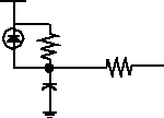
valid level. In this situation, it is recommended that you
use the external RC circuit. The RC delay should exceed
the time period it takes Vdd to reach a valid operating
Note:Ripple counter is 10 bits for Power on Reset (POR)
only.
Figure 12-1. Block Diagram of On-Chip Reset Circuit
POR
BROWN-OUT
MIWU
MCLR
wdt_time_out
10-Bit Asynch
Ripple
Counter
(DRT Start-Up
Timer)
Vdd
rc_clk
drt_time
_out
S
R
Q
QN
RESET
POR
enable
Figure 12-2. Time-Out Sequence on Power-Up
(MCLR not tied to Vdd)
Figure 12-3. Time-out Sequence on Power-up
(MCLR tied to Vdd): Slow Rise Time
Figure 12-4. External Power-On Reset Circuit
(For Slow Vdd Power-up)
Figure 12-5. Time-out Sequence on Power-up
(MCLR tied to Vdd): Fast Vdd Rise Time
Vdd
MCLR
POR
drt_time_out
RESET
Tdrt
Vdd
MCLR
POR
drt_time_out
RESET
Tdrt
V1
Vdd
R
C
MCLR
D
R1
Vdd
MCLR
POR
drt_time_out
RESET
Tdrt


