© 2000 Scenix Semiconductor, Inc. All rights reserved.
- 29 -
www.scenix.com
SX48BD/SX52BD/SX52BD75/SX52BD100
10.0
MULTI-FUNCTION TIMERS
The device contains two independent 16-bit multi-func-
tion timers, designated T1 and T2. These versatile, pro-
grammable timers reduce the software burden on the
CPU in real-time control applications such as PWM gen-
eration, motor control, triac control, variable-brightness
display control, sine wave generation, and data acquisi-
tion.
Each timer consists of a 16-bit counter register supported
by a dedicated 16-bit capture register and two 16-bit
comparison registers. The second compare register can
also serve as capture register. Each timer uses up to four
I/O pins: one clocking input, two capture inputs, and one
timer output. The timer I/O pins are alternate functions of
Port B pins for timer T1 and Port C pins for Timer T2.
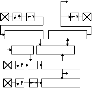
Figure10-1 is a block diagram showing the registers and
I/O pins of one timer. The 16-bit free-running
timer/counter register is initialized to 0000h upon reset
and counts upward continuously. It is clocked either by
an external signal provided on an I/O pin or by the on-
chip system clock divided by a 3-bit divide-by factor.
The CPU can access the Compare and Capture registers
by using the “mov !RB,W” instruction for T1 or the “mov
!RC,W” instruction for T2. The other timer registers are
not directly accessible.
You can configure the timer to generate an interrupt upon
overflow from FFFFh to 0000h, upon a match between
the counter value and a programmed comparison value,
or upon the occurrence of a valid capture signal on either
of two capture inputs.
The timers can be cleared to 0000h by writing to the reg-
isters accessed via MODE address $10. Clearing the
timer forces it to begin compare with R1.
The MODE register controls access to the timer regis-
ters. Because the MODE register is not memory mapped,
it is accessed by the following special purpose insteruc-
tions:
• mov M, #lit (move literal to lower 4-bits of MODE regis-
ter)
• mov M,W (move W to lower 5-bits of MODE register)
• mov W,M (move MODE register to W)
The value contained in the MODE register determines
which timer register is accessed by the “mov !rx,W”
instruction as indicated in Table10-1.
10.1
Timer Registers
Each timer consists of several registers.
Timer T1 registers:
T1CPL - Lower byte of Timer T1 capture register
T1CPH - Higher byte of Timer T1 capture register
T1R1CML - Lower byte of Timer T1 compare register 1
T1R1CMH - Higher byte of Timer T1 compare register 1
T1R2CML - Lower byte of Timer T1 compare register 2
T1R2CMH - Higher byte of Timer T1 compare register 2
T1CNTA - Timer T1 control register A
T1CNTB - Timer T1 control register B
Timer T2 registers:
T2CPL - Lower byte of Timer T2 capture register
T2CPH - Higher byte of Timer T2 capture register
T2R1CML - Lower byte of Timer T2 compare register 1
T2R1CMH - Higher byte of Timer T2 compare register 1
T2R2CML - Lower byte of Timer T2 compare register 2
T2R2CMH - Higher byte of Timer T2 compare register 2
T2CNTA - Timer T1 control register A
T2CNTB - Timer T1 control register B
Figure 10-1. Multi-Function Timer Block Diagram
Ext. Clock
Capture 1
Capture 2
3-Bit Divide-By
16-Bit Free-Running
16-Bit Comparator
Compare Register R1
Compare R2/Capture Register2
Timer/Counter
16-Bit Capture Register 1
MUX
match
Output
Compare Interrupt
System
Clock
Capture Interrupt
16-Bit
16-Bit
