© 2000 Scenix Semiconductor, Inc. All rights reserved.
- 25 -
www.scenix.com
SX48BD/SX52BD/SX52BD75/SX52BD100
8.0
OSCILLATOR CIRCUITS
The device supports several user-selectable oscillator
modes. The oscillator modes are selected by program-
ming the appropriate values into the FUSE Word register.
These are the different oscillator modes offered:
8.1
XT, LP or HS modes
In XT, LP or HS modes, you can use either an external
crystal/resonator network or an external clock signal as
the device clock.
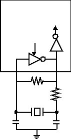
To use an external crystal/resonator network, you con-
nect a crystal or ceramic resonator to the OSC1/CLKIN
and OSC2/CLKOUT pins according to the circuit configu-
ration shown in Figure8-1. A parallel resonant funda-
mental crystal type is recommended. Use of a series
resonant crystal may result in a frequency that is outside
the crystal manufacturer specifications. For operating fre-
quencies above 50 MHz, HS3 setting must be selected
(FOSC2:FOSC0 should contain 110) and external clock
oscillators must be used. In addition, the bit 4
(XTLBUF_EN) of the FUSE Word register must be ini-
tialed to 0. In such cases, the clock oscillator output can
be directly connected to the OSC1 pin and the OSC2 pin
should be left open.Table 8-1 shows the external compo-
nent values associated with a crystal-based oscillator
(internal feedback resistor is disable through bit 6 of the
FUSE Word register - IFBD = 0).
If the XT, LP, or HS mode is selected, the OSC1/CLKIN
pin can be driven by an external clock source rather than
a resonator network, as long as the clock signal meets
the specified duty cycle, rise and fall times, and input lev-
els (Figure8-2). In this case, the OSC2/CLKOUT pin
should be left open.
LP: Low Power Crystal
XT: Crystal/Resonator
HS: High Speed Crystal/Resona-
tor/Clock Oscillator
RC: External Resistor/Capacitor
Internal Resistor/Capacitor
Table 8-1. External Component Selection for Crystal Oscillator (Vdd = 5.0V)
FOSC2:FOSC0
Crystal
Frequency
Setting
Symbol
C1 (pF)
C2 (pF)
RF (M)
Rs (Ohm)
011
4 MHz
XT2
33
56
1
0
011
8 MHz
XT2
22
56
1
0
100
20 MHz
HS1
22
33
1
0
101
32 MHz
HS2
15
47
1
0
101
50 MHz
HS2
15
33
1
0
Figure 8-1. Crystal Operation (or Ceramic Resonator)
(HS, XT or LP OSC Configuration)
SX Device
RF
XTAL
OSC2
OSC1
C1
C2
Internal
Circuitry
SLEEPCLK
RS
Figure 8-2. External Clock Input Operation
(HS, XT or LP OSC Configuration)
OSC1
OSC2
SX Device
Externally
Generated Clock
Open

