© 2000 Scenix Semiconductor, Inc. All rights reserved.
- 19 -
www.scenix.com
SX48BD/SX52BD/SX52BD75/SX52BD100
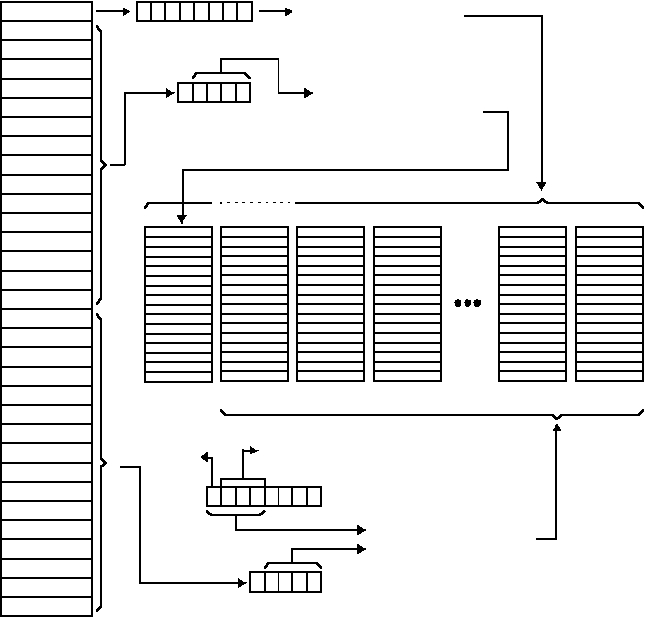
Figure 5-1. Register Access Modes
00h
01h
02h
03h
04h
05h
06h
07h
08h
09h
0Ah
0Bh
0Ch
0Dh
0Eh
0Fh
10h
11h
12h
13h
14h
15h
16h
17h
18h
19h
1Ah
1Bh
1Ch
1Dh
1Eh
1Fh
Indirect Addressing
Direct Addressing
Semi-Direct Addressing
X X X X
FSR
5-Bit “fr” Value
of Instruction
FSR bits 7:0 select one of
the registers in the global
register set or a register
in Bank 1 through Bank
F. Bank 0 is not
accessible.
“fr” bits 3:0 select one of 15
registers in the global
register set. The FSR
register is ignored. Bank 0
through Bank F are not
accessible.
FSR bits 7:4 select one of
16 banks, and “fr” bits 3:0
select one of 16 registers
in that bank. The four
low-order bits of FSR are
ignored. All 256 registers
in Bank 0 through Bank F
are accessible. The
global registers are not
accessible.
Bank 0
Bank 1
Bank 2
Bank E
Bank F
F0
F1
F2
F3
F4
F5
F6
F7
F8
F9
FA
FB
FC
FD
FE
FF
E0
E1
E2
E3
E4
E5
E6
E7
E8
E9
EA
EB
EC
ED
EE
EF
10
11
12
13
14
15
16
17
18
19
1A
1B
1C
1D
1E
1F
20
21
22
23
24
25
26
27
28
29
2A
2B
2C
2D
2E
2F
00
01
02
03
04
05
06
07
08
09
0A
0B
0C
0D
0E
0F
00 INDF
01 RTCC
02 PC
03 STATUS
04 FSR
05 RA
06 RB
07 RC
08 RD
09 RE
0A
0B
0C
0D
0E
0F
Global
Registers
fr
1
fr
0
User
Configured
Modified by BANK instruction
FSR
