© 2000 Scenix Semiconductor, Inc. All rights reserved.
- 10 -
www.scenix.com
SX48BD/SX52BD/SX52BD75/SX52BD100
For example, suppose all four Port A pins are configured
as outputs. To make RA0 and RA1 high and the remain-
ing Port A pins low, you could use the following code:
The second “mov” instruction in this example writes the Port
A data register (RA), which controls the output levels of the
Port A pins, RA0 through RA7. Note that Port A has only
four I/O pins in the 48-pin version of the device, in which
case only the four least significant bits of this register are
used.
When a write is performed to a port bit position that has
been configured as an input, a write to the port data register
is still performed, but it has no immediate effect on the pin. If
later that pin is configured to operate as an output, it will
reflect the value that has been written to the data register.
In the default device configuration, when a read is per-
formed from a port bit position, the operation is actually
reading the voltage level on the pin itself, not necessarily the
bit value stored in the port data register. This is true whether
the pin is configured to operate as an input or an output.
Therefore, with the pin configured to operate as an input,
the data register contents have no effect on the value that
you read. With the pin configured to operate as an output,
what is read generally matches what has been written to the
register. PORTRD of the T2CNT2 register determines how
the device reads data from its I/O ports (Port A through Port
E). Clear this bit to 0 to have the device read data from the
port I/O pins directly. Set this bit to 1 to have the device read
data from the port data registers. Under normal conditions, it
should not matter which method you use to read the port
data. However, if a port pin is configured as an output and
an external circuit forces the pin to the opposite value, the
value read from the port will depend on the reading mode
used. Note that this control bit is not related to multi-function
timers T1 and T2.
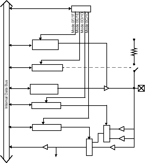
Figure 3-2. Port B, Port C, Port D, Port E Configuration
MODE
RB/RC/RD/RE
PLP_B/C/D/E
LVL_B/C/D/E
0 = Output
1 = Hi-Z Input
0 = Pullup Enable
1 = Pullup Disable
0 = CMOS Levels
1 = TTL Levels
RD
Port B: Input, MIWU, Comparator, Timer T1
Vdd
Pullup Resistor
(~20kW)
Port
M
U
X
ST_B/C/D/E
RD/WR
0 = Schmitt Trigger Enable
1 = Schmitt Trigger Disable
Port C: Input, Timer T2
TTL Buffer
CMOS Buffer
M
U
X
Pin
Schmitt Trigger Buffer
Direction
RB/RC/RD/RE
Data
~~
RD/WR
RD/WR
RD/WR
RD/WR
Port D and E: Input only
mov W,#$03
;load W with the value 03h
;(bits 0 and 1 high)
mov $05,W
;write 03h to Port A data
;register
