2
' 1999 Scenix Semiconductor, Inc. All rights reserved.
www.scenix.com
Device Configuration Options
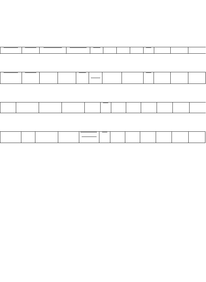
The register formats are shown in Figure 1 and the configuration fields within the registers are
explained in Table 2 through Table 5. Note that the register formats vary, depending on the SX
datecode variations. .
External Crystal/Resonator (XT, LP, or HS Mode)
SX18/20/28AC devices with datecode Axyywwxx (new revision) support extended crystal/resonator
modes. Table 3 shows the different mode being supported. The new version of the device has improved
internal crystal/resonator support circuitry. The external component values associated with oscillator
circuit may have to chnage when using the new version. The oscillator circuit is currently being
characterized. Contact Scenix for the component values.
Figure 1 Device Configuration Register Formats
FUSE Word for SX18/20/28AC Devices with Datecode yywwxx (old revisions)
FUSE Word for SX18/20/28AC Devices with Datecode Axyywwxx (new revision)
FUSEX Word for SX18/20/28AC Devices with Datecode yywwxx (old revisions)
FUSEX Word for SX18/20/28AC Devices with Datecode Axyywwxx (new revision)
TURBO
SYNC
OPTIONX
STACKX
IRC
DIV2
DIV1
DIV0
CP
WDTE
FOSC1
FOSC0
Bit 11
Bit 0
TURBO
SYNC
Reserved Reserved
IRC
DIV1/
IFBD
DIV0/
FOSC2
Reserved
CP
WDTE
FOSC1
FOSC0
Bit 11
Bit 0
IRCTRI
M2
PINS
IRCTRIM1
IRCTRIM0
Reserved
CF
BOR1
BOR0
RAM1
RAM0
MEM1
MEM0
Bit 11
Bit 0
IRCTRIM2
PINS
IRCTRIM1
IRCTRIM0
OPTIONX/
STACKX
CF
BOR1
BOR0
BORTR
IM1
BORTR
IM0
BP1
BP0
Bit 11
Bit 0
