© 2000 Scenix Semiconductor, Inc. All rights reserved.
- 7 -
www.scenix.com
SX18AC/SX20AC/SX28AC/SX18AC75/SX20AC75/SX28AC75
3.0 PORT DESCRIPTIONS
The device contains a 4-bit I/O port (Port A) and two 8-bit
I/O ports (Port B, Port C). Port A provides symmetrical
drive capability. Each port has three associated 8-bit reg-
isters (Direction, Data, TTL/CMOS Select, and Pull-Up
Enable) to configure each port pin as Hi-Z input or output,
to select TTL or CMOS voltage levels, and to enable/dis-
able the weak pull-up resistor. The upper four bits of the
registers associated with Port A are not used. The least
significant bit of the registers corresponds to the least
significant port pin. To access these registers, an appro-
priate value must be written into the MODE register.
Upon power-up, all bits in these registers are initialized to
“1”.
The associated registers allow for each port bit to be indi-
vidually configured under software control as shown
below:
3.1 Reading and Writing the Ports
The three ports are memory-mapped into the data mem-
ory address space. To the CPU, the three ports are avail-
able as the RA, RB, and RC file registers at data memory
addresses 05h, 06h, and 07h, respectively.
Writing to a port data register sets the voltage levels of
the corresponding port pins that have been configured to
operate as outputs. Reading from a register reads the
voltage levels of the corresponding port pins that have
been configured as inputs.
Table 3-1. Port Configuration
Data Direction
Registers:
RA, RB, RC
TTL/CMOS
Select Registers:
LVL_A, LVL_B,
LVL_C
Pullup Enable
Registers:
PLP_A, PLP_B,
PLP_C
0
1
0
1
0
1
Output
Hi-Z
Input
CMOS
TTL
Enable
Disable
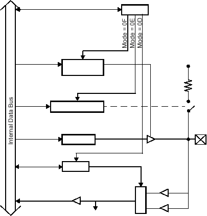
Figure 3-1. Port A Configuration
MODE
RA
RA Data
LVL_A
0 = Output
1 = Hi-Z Input
WR
WR
0 = CMOS
1 = TTL
RD
TTL Buffer
CMOS Buffer
Vdd
Pullup
Port A PIN
M
U
X
WR
Direction
PLP_A
0 = Pullup Enable
1 = Pullup Disable
Port A INPUT
WR
