© 2000 Scenix Semiconductor, Inc. All rights reserved.
- 28 -
www.scenix.com
SX18AC/SX20AC/SX28AC/SX18AC75/SX20AC75/SX28AC75
Figure 12-3 shows the on-chip Power-On Reset
sequence where the MCLR and Vdd pins are tied
together. The Vdd signal is stable before the DRT time-
out period expires. In this case, the device will receive a
proper reset. However, Figure 12-4 depicts a situation
where Vdd rises too slowly. In this scenario, the DRT will
time-out prior to Vdd reaching a valid operating voltage
level (Vdd min). This means the device will come out of
reset and start operating with the supply voltage not at a
valid level. In this situation, it is recommended that you
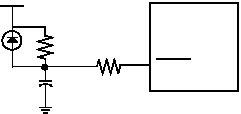
use the external RC circuit shown in Figure 12-5. The RC
delay should exceed the time period it takes Vdd to reach
a valid operating voltage
Note 1: The external Power-On Reset circuit is required
only if Vdd power-up is too slow. The diode D helps dis-
charge the capacitor quickly when Vdd powers down.
Note 2: R < 40 kW is recommended to make sure that
voltage drop across R does not violate the device electri-
cal specifications.
Note 3: R1 = 100W to 1kW will limit any current flowing
into MCLR from external capacitor C. This helps prevent
MCLR pin breakdown due to Electrostatic Discharge
(ESD) or Electrical Overstress (EOS).
13.0 BROWN-OUT DETECTOR
The on-chip brown-out detection circuitry resets the
device when Vdd dips below the specified brown-out volt-
age. The device is held in reset as long as Vdd stays
below the brown-out voltage. The device will come out of
reset when Vdd rises above the brown-out voltage. The
brown-out level is preset to approximately 4.2V at the
factory. The brown-out circuit can be disabled through
BOR0 and BOR1 bits contained in the FUSEX Word reg-
ister.
Figure 12-3. Time-out Sequence on Power-up
(MCLR tied to Vdd): Fast Vdd Rise Time
Figure 12-4. Time-out Sequence on Power-up
(MCLR tied to Vdd): Slow Rise Time
Vdd
MCLR
POR
drt_time_out
RESET
Tdrt
Vdd
MCLR
POR
drt_time_out
RESET
Tdrt
V1
Figure 12-5. External Power-On Reset Circuit
(For Slow Vdd Power-up)
Vdd
R
C
MCLR
D
R1


