© 2000 Scenix Semiconductor, Inc. All rights reserved.
- 21 -
www.scenix.com
SX18AC/SX20AC/SX28AC/SX18AC75/SX20AC75/SX28AC75
9.0 OSCILLATOR CIRCUITS
The device supports several user-selectable oscillator
modes. The oscillator modes are selected by program-
ming the appropriate values into the FUSE Word register.
These are the different oscillator modes offered:
9.1 XT, LP or HS modes
In XT, LP or HS, modes, you can use either an external
resonator network or an external clock signal as the
device clock.
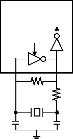
To use an external resonator network, you connect a
crystal or ceramic resonator to the OSC1/CLKIN and
OSC2/CLKOUT pins according to the circuit configura-
tion shown in Figure 9-1. A parallel resonant crystal type
is recommended. Use of a series resonant crystal may
result in a frequency that is outside the crystal manufac-
turer specifications. Table 9-1 shows the recommended
external components associated with a crystal-based
oscillator. Table 9-2 shows the recommended external
component values for a resonator-based oscillator.
Bits 0, 1 and 5 of the FUSE register (FOSC1:FOSC2) are
used to configure the different external resonator/crystal
oscillator modes. These bits allow the selection of the
appropriate gain setting for the internal driver to match
the desired operating frequency. If the XT, LP, or HS
mode is selected, the OSC1/CLKIN pin can be driven by
an external clock source rather than a resonator network,
as long as the clock signal meets the specified duty
cycle, rise and fall times, and input levels (Figure 9-2). In
this case, the OSC2/CLKOUT pin should be left open.
LP: Low Power Crystal
XT: Crystal/Resonator
HS: High Speed Crystal/Resonator
RC: External Resistor/Capacitor
Internal Resistor/Capacitor
Figure 9-1. Crystal Operation (or Ceramic Resonator)
(HS, XT or LP OSC Configuration)
Figure 9-2. External Clock Input Operation
(HS, XT or LP OSC Configuration)
SX Device
RF
XTAL
OSC2
OSC1
C1
C2
Internal
Circuitry
SLEEP
RS
Externally
Generated Clock
OSC1
OSC2
Open
SX Device
Table 9-1. External Component Selection for Crystal Oscillator(Vdd=5.0V)
FOSC2:FOSC0
Crystal
Frequency
C1
C2
RF
RS
010
4 MHz
15 pF
22 pF
1 MW
0 W
011
8 MHz
56 pF
33 pF
1 MW
0 W
011
20 MHz
33 pF
22 pF
1 MW
0 W
011
32 MHz
15 pF
22 pF
1 MW
0 W
100
50* MHz
15 pF
15 pF
1 MW
0 W
* 50 MHz fundamental crystal

