© 1999 Scenix Semiconductor, Inc. All rights reserved.
- 7 -
www.scenix.com
SX18AC / SX20AC / SX28AC
For example, suppose all four Port A pins are configured
as outputs and with RA0 and RA1 to be high, and RA2
and RA3 to be low:
The second “mov” instruction in this example writes the
Port A data register (RA), which controls the output levels
of the four Port A pins, RA0 through RA3. Because Port
A has only four I/O pins, only the four least significant bits
of this register are used. The four high-order register bits
are “don’t care” bits. Port B and Port C are both eight bits
wide, so the full widths of the RB and RC registers are
used.
When a write is performed to a bit position for a port that
has been configured as an input, a write to the port data
register is still performed, but it has no immediate effect
on the pin. If later that pin is configured to operate as an
output, it will reflect the value that has been written to the
data register.
When a read is performed from a bit position for a port,
the operation is actually reading the voltage level on the
pin itself, not necessarily the bit value stored in the port
data register. This is true whether the pin is configured to
operate as an input or an output. Therefore, with the pin
configured to operate as an input, the data register con-
tents have no effect on the value that you read. With the
pin configured to operate as an output, what is read gen-
erally matches what has been written to the register.
3.1.1 Read-Modify-Write Considerations
Caution must be exercised when performing two succes-
sive read-modify-write instructions (SETB or CLRB oper-
ations) on I/O port pin. Input data used for an instruction
must be valid during the time the instruction is executed,
and the output result from an instruction is valid only after
that instruction completes its operation. Unexpected
results from successive read-modify-write operations on
I/O pins can occur when the device is running at high
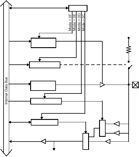
Figure 3-2. Port B, Port C Configuration
MODE
RB or RC
PLP_B or PLP_C
LVL_B or LVL_C
0 = Output
1 = Hi-Z Input
WR
0 = Pullup Enable
1 = Pullup Disable
WR
0 = CMOS
1 = TTL
RD
Port B: Input, MIWU, Comparator
Vdd
Pullup Resistor
(~20kW)
Port B or
M
U
X
WR
ST_B or ST_C
WR
0 = Schmitt Trigger Enable
1 = Schmitt Trigger Disable
Port C: Input Only
TTL Buffer
CMOS Buffer
M
U
X
Port C PIN
Schmitt Trigger Buffer
Direction
RB or RC
WR
Data
~~
mov
W,#$03
;load W with the value 03h
;(bits 0 and 1 high)
mov
$05,W
;write 03h to Port A data
;register
