78
www.ubicom.com
IP2022 Data Sheet
Figure 5-27 SRAM Chip Selection Equations
For zero wait-state access, the external memory must
meet the access time specification shown in Table 5-19.
Slower memories can be accommodated by programming
wait states in the EMCFG register. Software is
responsible for allowing the memory cycle to complete
before reading the DATAH/DATAL registers.
Note: Parallel Slave Peripheral and RB7:4 interrupts must
be disabled for external memory operations.
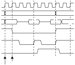
A read cycle to external memory has the timing shown in
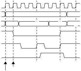
Figure 5-28. Write cycle timing is shown in Figure 5-29. All
external memory cycles are 16-bit transfers, with the low
byte (A0 = 0) followed by the high byte (A0 = 1).
Figure 5-28 Read Cycle
Figure 5-29 Write Cycle
EMBRT = System Clock [Hz] x Bus Release Time [ns] = Range 0 - 1 (truncated)
515-097.eps
Bus Release Timing:
109
Max BRT [ns] (SRAM chip spec.) = 2 x 10 = N ns (truncated)
System Clock [Hz]
9
EMRDT2:0 = System Clock [Hz] x Access Time [ns] (SRAM chip spec.) + 1 = Range 1 - 8 (truncated)
109
Read Access Time:
Cycles between IREAD and DATAH present (not including IREAD or DATAH access cycles) = Read Access Time + 1
Cycles between IREAD and DATAL present (not including IREAD or DATAL access cycles) = 2(Read Access Time + 1)
Cycles between consecutive IREADs (not including IREAD access cycles) = 2(Read Access Time + 1) + Bus Release Timing + 1
Table 5-19 SRAM Access Time Specification
CPU Core Clock Frequency
(MHz)
SRAM Access Time
(ns)
80
35
100
25
120
25
150
12/15/20*
* Depends on minimum WR pulse width specification.
RC7:0
RD7:0
LE (RB6)
System Clock
515-088c.eps
RD (RB5)
A0 (RB7)
ADDRH
ADDRL
DATAH
DATAL
ADDRH
ADDRL
IREAD
ADDRSEL
RC7:0
RD7:0
LE (RB6)
System Clock
515-089c.eps
WR (RB4)
A0 (RB7)
ADDRH
ADDRL
DATAH
DATAL
ADDRH
ADDRL
IWRITE
ADDRSEL

