IP2022 Data Sheet
www.ubicom.com
77
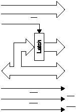
5.11 External Memory Interface
Port C and Port D can also be used for a parallel interface
for up to 128K bytes of linear-addressed external memory,
(not program memory) as shown in Figure 5-25. With
additional software-based addressing on I/O, up to 2M
bytes is possible. Port C implements the high address
bits, and Port D is multiplexed between data and the low
address bits. A level-triggered 8-bit latch (TI part number
SN74AC573 or equivalent) is required for demultiplexing.
Figure 5-25 External Memory Interface
External memory is accessed as 16-bit words at word-
aligned byte addresses 0x800000 to 0x81FFFE, as
shown in Figure 5-26. External 8-bit memory can only be
accessed through the current ADDRX/ADDRH/ADDRL
pointer
using
the
iread/ireadi
and
iwrite/iwritei
instructions. Programs cannot
execute directly out of external memory, and commands
on the ISD/ISP interface cannot directly access external
memory. Like data memory, however, external memory
can be accessed over the ISD/ISP interface by executing
instructions which move data between memory and the W
register.
5.11.1 EMCFG Register
See Section 7.1.4 for information about the EMCFG
register.
Note: When external memory is enabled (EMEN = 1), the
RDDIR register value is overridden. PSP function will
need to be disabled. Port B bits 4-7 (WR, RD, LE and A0
respectively) need to be configured in software, which
includes disabling any interrupts.
Note: Wait 1 cycle after changing ADDRX bit 7,
ADDRSEL or EMCFG bit 7 before executing fread,
fwrite, ferase, iread, iwrite, ireadi or
iwritei.
Figure 5-26 External Memory Map
Software is responsible for inserting a one-instruction
delay between changing the address (i.e. the contents of
the ADDRSEL, ADDRX, ADDRH, or ADDRL registers)
and
executing
the
iread/ireadi
or
iwrite/iwritei instruction, if required by the timing
of the external latch. Figure 5-27 shows the calculations
used to help select the correct SRAM chip.
IP2022
WR
External
Memory
515-087.eps
RD
A0
A8:1
A0
D7:0
LE
A16:9
RD
WR
Address
Data
Addr
RB6
RB7
RD7:0
RC7:0
RB5
RB4
515-090a.eps
Program RAM
Reserved
0x000000
7
0
0x004000
Flash Program Memory
0x01FFFE
0x010000
Byte
Address
0x003FFE
0x00FFFE
Reserved
0x020000
External Memory
0x800000
0x7FFFFE
0x81FFFE
