IP2022 Data Sheet
www.ubicom.com
71
5.9
Linear Feedback Shift Register
Four linear feedback shift register (LFSR) units provide
hardware support for the computation-intensive inner
loops
of
algorithms
commonly
used
in
data
communications, such as:
•
Cyclic Redundancy Check (CRC)
•
Data Scrambling
•
Data Whitening
•
Encryption/Decryption
•
Hashing
The LFSR units implement a programmable architecture,
which can be adapted for algorithms used by the
Bluetooth, Ethernet, Homeplug, HomePNA, HomeRF,
IEEE 802.11, and USB communication protocols. Figure
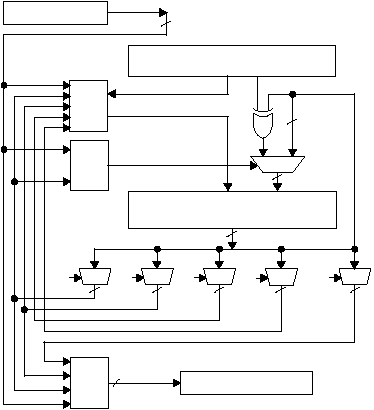
5-18 is a block diagram of the LFSR architecture.
Figure 5-18 LFSR Block Diagram
The 40-bit residue register and its surrounding circuits are
the computational core of an LFSR unit. On every clock
cycle, 39 output bits from the register are available at the
input for performing a shift operation or a polynomial
add/subtract-and-shift operation. Four 40-bit multiplexers
at the output of the residue register allow selecting up to
four terms of the register for feedback into the input (D0),
polynomial operation control (POLY_XOR_EN), and
output (DOUT) bit streams. A fifth multiplexer is only used
for generating the output bit stream.
The polynomial and residue registers are mapped as five
8-bit registers. The mapping of the residue register is
controlled by the ML_OUT bit of the LFSRCFG3 register,
as shown in Figure 5-19.
Figure 5-19 Mapping of the Residue Register
Polynomial Register (POLYx)
Residue Register (RESx)
1..39
1..39
0..39
0
0
0
1
0..38
0..39
FB1
40:1
0..39
FB2
40:1
0..39
FB3
40:1
0..39
DOUT
40:1
D0
Source
Gating
POLY
Source
Gating
DOUT
Source
Gating
16-bit DATAOUT Register
DATAIN Register
515-082a.eps
D0
POLY_XOR_EN
DOUT
DIN
0..39
FB4
40:1
40
39
39
1
1
1
1
1
1
1
515-083.eps
RES4
7
0
RES3
7
0
RES2
7
0
RES1
7
0
RES0
7
0
0
Residue Register (ML_OUT = 0)
39
39
Residue Register (ML_OUT = 1)
0