IP2022 Data Sheet
www.ubicom.com
51
5.4
Multi-Function Timers (T1 and T2)
The IP2022 contains two independent 16-bit multi-
function timers, called T1 and T2. These versatile,
programmable timers reduce the software burden on the
CPU in real-time control applications such as PWM
generation, motor control, triac control, variable-
brightness display control, sine-wave generation, and
data acquisition.
Each timer consists of a 16-bit counter register supported
by a dedicated 16-bit capture register and two 16-bit
compare registers. The second compare register can also
serve as capture register. Each timer may use up to four
external pins: TxCPI1 (Capture Input), TxCPI2 (Capture
Input), TxCLK (Clock Input), TxOUT (Output). These pins
are multiplexed with general-purpose I/O port pins. The
port direction register has priority over the timer
configuration, so the port direction register must be
programmed appropriately for each of these four signals
if their associated timer functions are used.
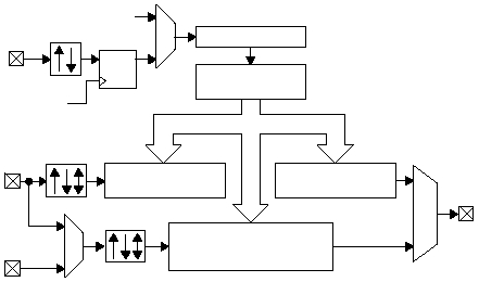
Figure 5-5 is a block diagram showing the registers and
I/O pins of one timer. Each timer is based on a 16-bit
counter/timer driven by a 15-bit prescaler. The input of the
prescaler can be either the system clock or an external
clock signal which is internally synchronized to the system
clock. The counter cannot be directly written by software,
but it may be cleared by writing to the TxRST bit in the
TxCTRL register.
Figure 5-5 Multifunction Timer Block Diagram
5.4.1
Timers T1, T2 Operating Modes
Each timer can be configured to operate in one of the
following modes:
•
Pulse-Width Modulation (PWM)
•
Timer
•
Capture/Compare
PWM Mode
In PWM Mode, the timer can generate a pulse-width
modulated signal on its output pin, TxOUT. The period of
the PWM cycle (high + low) is specified by the value in the
TxCAP2H/TxCAP2L register. The high time of the pulse is
specified by the value in the TxCMP1H/TxCMP1L
register.
PWM mode can be used to generate an external clock
signal that is synchronous to the IP2022 system clock. For
example, by loading TxCMP1H/TxCMP1L with 1 and
TxCAP2H/TxCAP2L with 2, a symmetric 50-MHz external
clock can be generated from a 120 MHz system clock. In
some applications, this can eliminate crystals or
oscillators required to produce clock signals for other
components in the system.
The 16-bit counter/timer counts upward. After reaching
the value stored in the TxCMP1H/TxCMP1L register
minus one, at the next clock edge the TxOUT pin is driven
low. The counter/timer is unaffected by this event and
continues to increment. After reaching the value stored in
the TxCAP2H/TxCAP2L register minus one, at the next
clock edge the timer is cleared. When the counter is
515-005.eps
TxCPI1
TxCAP1H/TxCAP1L
Register
TxOUT
TxCMP1H/TxCMP1L
Register
TxCLK
D Q
TxCPI2
TxCAP2H/TxCAP2L
or TxCMP2H/TxCMP2L
Register
TxCNTH/TxCNTL
Register
15-Bit Prescaler
System
Clock
System
Clock
