IP2022 Data Sheet
www.ubicom.com
47
5. NOP
6. Enable the interrupt input(s) by setting the corre-
sponding bit(s) in the INTE register.
7. Set the GIE bit.
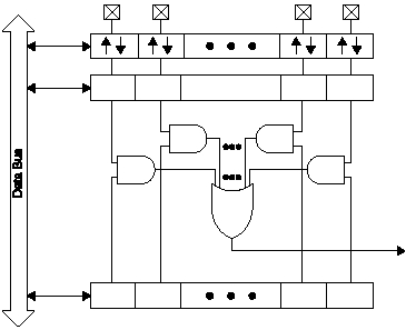
Figure 5-2 shows the Port B interrupt logic. Port B has
three registers for supporting external interrupts, the
INTED (Section 5.1.6), INTF (Section 5.1.7), and INTE
(Section 5.1.8) registers. The INTED register controls the
logic which selects the edge sensitivity (i.e. rising or falling
edge) of the Port B pins. When an edge of the selected
type occurs, the corresponding flag in the INTF register is
set, whether or not the interrupt is enabled. The interrupt
signal passed to the system interrupt logic is the OR
function of the AND of each interrupt flag in the INTF
register with its corresponding enable bit in the INTE
register. See Section 5.1.8.
Figure 5-2 Port B Interrupt Logic
5.1.2
Reading and Writing the Ports
The port registers are memory-mapped into the data
memory address space between 0x020 and 0x03A. In
addition, Port B has three extra registers located between
0x017 and 0x019 which are used to support external
interrupt inputs.
Generally, successive read and write operations on the
same I/O port is not an issue, as there are separate IN an
OUT registers for each I/O port. Care must be given to
ensure that enough time is allowed for data written to the
OUT register can propogate to the IN register on a given
port. If this is an issue, 2 nop instructions (or 3 nop
instructions if the SYNC bit in the FUSE1 register is clear)
should be inserted between any read-modify-write
instruction sequences.
5.1.3
RxIN Registers
The RxIN registers are virtual registers that provide read-
only access to the physical I/O pins. Reading these
registers returns the states on the pins, which may be
driven either by the IP2022 or an external device. If the
SYNC bit in the FUSE1 register is clear, the states are
read from a synchronization register. If an application
reads data from a device running asynchronously to the
IP2022, the SYNC bit should be cleared to avoid the
occurrence of metastable states (i.e. corrupt data caused
by an input which fails to meet the setup time before the
sampling clock edge, which theoretically could interfere
with the operation of the CPU).
5.1.4
RxOUT Registers
The RxOUT registers are data output buffer registers. The
data in these registers is driven on any I/O pins that are
configured as outputs. On reads, the RxOUT registers
RB7
INTED Register
515-031.eps
RB6
RB1
RB0
INTF Register
INTE Register
Port B
Interrupt
