46
www.ubicom.com
IP2022 Data Sheet
5.0 Peripherals
The IP2022 provides an array of on-chip peripherals
needed to support a broad range of embedded Internet
applications:
•
2 Serializer/Deserializer (SERDES) units
•
Real-time timer
•
T0 timer
•
2 General-purpose timers with compare and capture
Registers
•
Watchdog timer
•
10-bit, 8-channel A/D converter
•
Analog comparator
•
Parallel slave peripheral interface
All of the peripherals except the Watchdog Timer and the
Real-Time Timer use alternate functions of the I/O port
pins to interface with external signals.
5.1
I/O Ports
The IP2022 contains one 4-bit I/O port (Port A) and six 8-
bit I/O ports (Port B through Port G). The four Port A pins
have 24 mA current drive capability. All the ports have
symmetrical drive. Inputs are 5V-tolerant. Outputs can
use the same 2.3–2.7V power supply used for the CPU
core and peripheral logic, or they can use a higher voltage
(up to 3.6V). The IOVdd pins are provided for the I/O port
pin output drivers. Port G has a separate GVdd pin which
can be used to run the Port G output drivers at a voltage
different from that used for the other ports, since Port G
must run from a 2.3–2.7V power supply.
Each port has separate input (RxIN), output (RxOUT),
and direction (RxDIR) registers, which are memory
mapped. The numbers in the pin names correspond to the
bit positions in these registers. These registers allow each
port bit to be individually configured as a general-purpose
input or output under software control. Unused pins
should be configured as outputs, to prevent them from
floating. Port B has three additional registers for
supporting external interrupts (see Section 5.1.1).
Each port pin has an alternate function used to support
the on-chip hardware peripherals, as listed in Table 2-1.
Port A and Port B support the multi-function timers Timer
1 and Timer 2. Port B, Port C, and Port D support the
Parallel Slave Peripheral (PSP) and external memory
functions.
Port
E
and
Port
F
support
the
serializer/deserializer (SERDES) units. Port G supports
the analog to digital converter (ADC) and the analog
comparator. Before enabling a hardware peripheral,
configure the port pins for input or output as required by
the peripheral.
Note: There is positive-feedback circuitry present on the
I/O ports when configured as input. This causes an input
that was previously high, then subsequently tri-stated (i.e.
not driven), to be actively driven by the IP2022 to a
voltage level of approximately 1.7V, or mid-supply
(IOVDD).
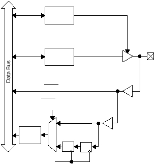
Figure 5-1 shows the internal hardware structure and
configuration registers for each pin of a port.
Figure 5-1 Port Pin Block Diagram
5.1.1
Port B Interrupts
Any of the 8 Port B pins can be configured as an external
interrupt input. Logic on these inputs can be programmed
to sense rising or falling edges. When an edge is
detected, the interrupt flag for the port pin is set.
The recommended initialization sequence is:
1. Configure the port pins used for interrupts as inputs
by programming the RBDIR register.
2. Be sure all enabled interrupt pins are driven to valid
logic levels, not floating.
3. Select the desired edge for triggering the interrupt
by programming the INTED register. This may set
interrupt flags.
4. Clear the interrupt flags in the INTF register.
515-030a.eps
Port Pin
RxDIR
Register
RxIN Register
(SYNC bit set)
0 = Output
1 = Hi-Z Input
RxOUT
Register
RxIN
Register
M
U
X
1
0
SYNC bit
(FUSE1)
FF
FF
Core Clock
