26
www.ubicom.com
IP2022 Data Sheet
3.9
Clock Oscillator
There are two clock oscillators, the OSC oscillator and the
RTCLK oscillator. The OSC oscillator is capable of
operating at 3MHz to 5MHz using an external crystal or
ceramic resonator. Using the PLL clock multiplier, the
OSC clock is intended to provide the time base for running
the CPU core at speeds up to 120MHz. The RTCLK
oscillator operates at 32.768kHz using an external crystal.
This oscillator is intended for running the real-time timer
when the OSC oscillator and PLL clock multiplier are
turned off. Either clock source can be driven by an
external clock signal, up to 120MHz for the OSC1 input
and up to 120MHz for the RTCLK1 input.
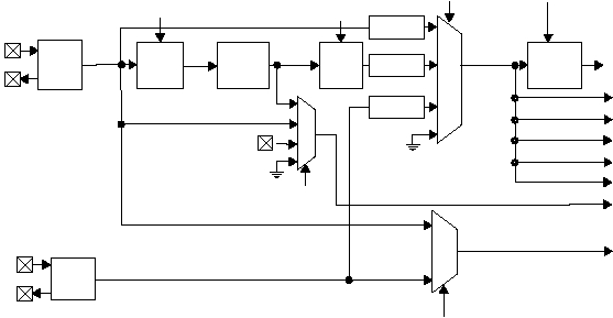
Figure 3-16 shows the clock logic. The PLL clock
multiplier has a fixed multiplication factor of 50. The PLL
is preceded by a divider capable of any integer divisor
between 1 and 8, as controlled by the PIN2:0 bits of the
FUSE0 register. The PLL is followed by a second divider
capable of any integer divisor between 1 and 4, as
controlled by the POUT1:0 bits of the FUSE0 register. A
third divider which only affects the clock to the CPU core
is controlled by the speed change mechanism described
in Section 3.4. If both the OSC oscillator and PLL are re-
enabled simultaneously, the delay is controlled by only the
FUSE0 WUDP2:0 bits. The system clock suspend time
during wakeup from clock stop mode (SLEEP), when
INTSPD is loaded into SPDREG from Port B interrupt or
RTTMR interrupt is specified by the FUSE0 WUDX2:0
bits. See Section 3.10.1 for a description of the FUSE0
WUDX2:0 and WUDP2:0 bits.
Note: Bits in the FUSE0 register are flash memory cells
which cannot be changed dynamically during program
execution.
Figure 3-16 Clock Logic
515-002f.eps
Timer 1
Timer 0
CPU Core
0 - 120MHz
Timer 2
RTTMR
SERDES
Clock
SPDREG
Divider
Post-
Scaler
Pre-
Scaler
RTCLK
Driver
RTCLK1
RTCLK2
50X PLL
Clock
Multiplier
OSC
Driver
OSC1
OSC2
System
Clock
0 - 120
MHz
PLL Bypass
External Memory Logic
Crystal 3 - 5 MHz
Ext. 0 - 120 MHz
Crystal 32.768 kHz
Ext. 0 - 120 MHz
3 - 5
MHz
FUSE0
Register
(bits 11:9)
FUSE0
Register
(bits 13:12)
50 - 300
MHz
speed
Instruction
speed
Instruction
0 - 120
MHz
RTCFG Register, RTSS bit
SxMode Register
(CLKS1:0)
ADC
WUDX2:0
WUDP2:0
WUDX2:0
SxCLK
