12
www.ubicom.com
IP2022 Data Sheet
3.0 System Architecture.
The IP2022 CPU executes from a 32K × 16 flash program
memory and an 8K × 16 RAM program memory. Figure 3-
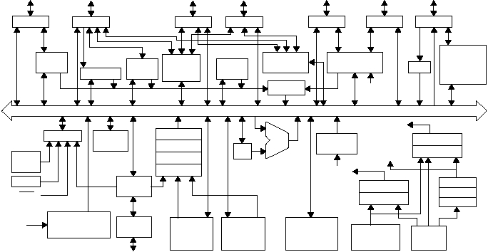
1 shows the IP2022 detailed block diagram. The
maximum execution rate is 30 MIPS from flash and 120
MIPS from RAM. Speed-critical routines can be copied
from the flash memory to the RAM for faster execution.
The CPU operates on 8-bit data in 128 special-purpose
registers, 128 global registers, and 3840 bytes of data
memory. The special-purpose registers hold control and
status bits used for CPU control and for interface with
hardware peripherals (timers, I/O ports, A/D converter,
etc.)Although the philosophy followed in the design of
Ubicom products emphasizes the use of fast RISC CPUs
with predictable execution times to emulate peripheral
devices in software (the ipModule™ concept), there are a
few hardware peripherals which are difficult to emulate in
software alone (e.g. an A/D converter) or consume an
excessive number of instruction cycles when operating at
high speed (e.g. data serialization/deserialization). The
design of the IP2022 incorporates only those hardware
peripherals which can greatly accelerate or extend the
reach of the ipModule™ concept. The hardware
peripherals included on-chip are:
•
52 I/O port pins
•
Watchdog timer
•
Real-time timer
•
2 Multifunction 16-bit timers with compare and cap-
ture registers
•
2 Real-time 8-bit timers
•
2 Serializer/deserializer (SERDES) units
•
4 Linear feedback shift register (LFSR) units
•
10-bit, 8-channel A/D converter
•
Analog comparator
•
Parallel slave peripheral interface
There is a single interrupt vector which can be
reprogrammed by software. On-chip peripherals and up to
8 external inputs can raise interrupts.
There are five sources of reset:
•
RST external reset input
•
Power-On Reset (POR) logic
•
Brown-Out Reset (BOR) logic (detects low AVdd con-
dition)
Figure 3-1 IP2022 Detailed Block Diagram
Internal Data Bus
Port A
RTCLK
SxCLK
Real-Time
Clock Driver
OSC
Driver
Timer 1
(T1)
Port E
Port F
Port G
(2) Serializer/
Deserializers
Analog
Comparator,
2x Ethernet
Squelch
Timer 2
(T2)
Port B
Timer 0
(T0)
Interrupt
Port D
Port C
Edge Det.
Parallel
Slave
Peripheral
ADC
Multiplexer
Divider
CPU Core Clock
Multiplexer
Divider
PLL
Divider
Divider
4KB Data
Memory
515-038a.eps
System
Clock
Real-Time
Timer
Reset
W
ALU
Watchdog Timer
with Pre-Scaler
ISD
Writeback
ISP
Brown
Out
POR
RST
Execute
Decode
64KB Flash
Program
Memory
16KB RAM
Program
Memory
Fetch
Internal
RC
Clock
(4) LFSR
Units
Ext. Memory
Interface
