IP2022 Data Sheet
www.ubicom.com
109
9.2
µBGA
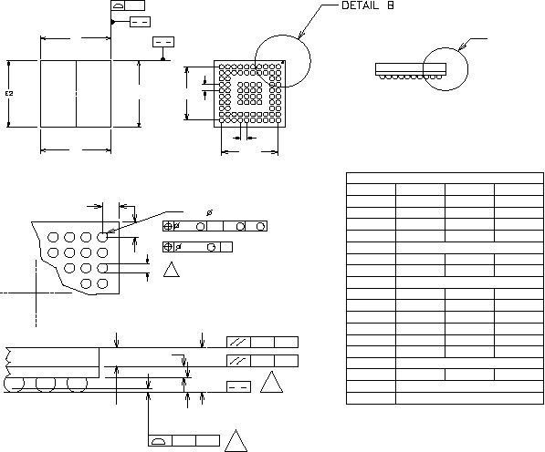
80-pin, 9 mm × 9 mm × 0.95 mm body, 0.8 mm ball spacing
REF.
A
A1
A2
D
D1
DIMENSIONAL REFERENCE
D2
E
E1
E2
b
c
aaa
bbb
ccc
e
f
M
N
0.80
0.90
10
80
0.80 BSC
8.80
0.39
9.00
0.44
0.25
7.20 BSC
0.12
0.10
0.10
1.00
9.20
0.49
9.00
9.00
9.00
9.20
9.20
9.20
8.80
8.80
8.80
0.65
0.70
0.75
0.21
0.26
0.31
1.11
1.21
1.31
MIN.
NOM.
MAX.
7.20 BSC
D
0.10
A
B
E
D2
TOP VIEW
BOTTOM VIEW
(E1)
e
e
(D1)
10
9
8
7
6
5
4
3
2
1
A
B
C
D
E
F
G
H
J
K
SIDE VIEW
DETAIL A
DETAIL B
f
f
b
4
NX
b
0.15
S
S
C
C
A
B S
S
0.075
DETAIL A
SEATING PLANE
A2
A1A
c
ccc
C
C
C
bbb
6
5
aaa
C
1. All Dimensins are in millimeters.
2. ’e’ represents the basic solder ball pitch.
3. ’M’ represents the basic solder ball matrix size, and
symbol ’N’ is the number of balls after depopulating.
4. ’b’ is measureable at the maximum solder ball diameter
after reflow parallel to primary datum - C - .
5. Dimension ’aaa’ is measured parallel to primary datum - C - .
6. Primary datum - C - and seating plane are defined by the
spherical crowns of the solder balls.
7. Package surface shall be matte finish charmilles 24 to 27.
8. package centering to substrate shall be 0.0760mm maximum
for both x and y direction respectively.
9. Package warp shall be 0.050mm maximum.
10. Substrate material base is BT resin.
11. The overall package thickness ’A’ already considers collapse balls.
12. Dimensioning and tolerancing per ASME Y14.5-1994.
