IP2022 Data Sheet
www.ubicom.com
81
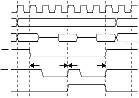
A read cycle to external memory has the timing shown in
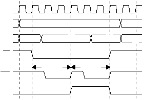
Figure 5-31. Write cycle timing is shown in Figure 5-32. All
external memory cycles are 16-bit transfers, with the low
byte (A0 = 0) followed by the high byte (A0 = 1).
Figure 5-31 Read Cycle
Figure 5-32 Write Cycle
5.11.1 EMCFG Register
Table 5-19 SRAM Access Time Specification
CPU Core Clock Frequency
(MHz)
SRAM Access Time
(ns)
80
35
100
25
120
25
150
12/15/20*
* Depends on minimum WR pulse width specification.
RC7:0
RD7:0
LE
Clock
515-088.eps
RD
A0
ADDRH
ADDRL
DATAH
DATAL
ADDRH
ADDRL
Taccess
Taccess
RC7:0
RD7:0
LE
Clock
515-089.eps
WR
A0
ADDRH
ADDRL
DATAH
DATAL
ADDRH
ADDRL
Taccess
Taccess
7
6
5
3
2
0
EMEN EMBRT
EMWRT2:0
EMRDT2:0
Name
Description
EMEN
Enable external memory interface
0 = Port C and Port D available for
general-purpose I/O
1 = Port C and Port D used for exter-
nal memory interface
EMBRT
Enable bus release wait state
0 = No wait state
1 = One wait state added between a
read cycle followed by a write
cycle
EMWRT2:0
WR pulse width, in CPU core clock cycles
000 = 1
001 = 2
010 = 3
011 = 4
100 = 5
101 = 6
110 = 7
111 = 8
EMRDT2:0
RD pulse width, in CPU core clock cycles
000 = 1
001 = 2
010 = 3
011 = 4
100 = 5
101 = 6
110 = 7
111 = 8

