80
www.ubicom.com
IP2022 Data Sheet
•
PSPEN1—set to enable Port C for data transfer, clear
to disable. (If this bit is set, the Parallel Slave Periph-
eral will immediately override the RCDIR register.)
•
PSPHEN—set to enable HOLD output, clear to dis-
able. (If this bit is set, the Parallel Slave Peripheral will
immediately override bit 5 of the RBDIR register.)
•
PSPRDY—set to release HOLD. This bit always
reads as 0.
5.11
External Memory Interface
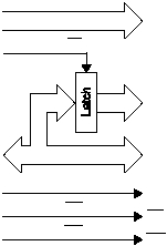
Port C and Port D can also be used for a parallel interface
for up to 128K bytes of external memory, as shown in
Figure 5-29. Port C implements the high address bits, and
Port D is multiplexed between data and the low address
bits. A level-triggered 8-bit latch (TI part number
SN74AC573 or equivalent) is required for demultiplexing.
Figure 5-29 External Memory Interface
External memory is accessed as 16-bit words at word-
aligned byte addresses 0x1000000 to 0x103FFFE, as
shown in Figure 5-30. External memory can only be
accessed through the current ADDRX/ADDRH/ADDRL
pointer
using
the
iread/ireadi
and
iwrite/iwritei instructions. Programs cannot
execute directly out of external memory, and commands
on the ISD/ISP interface cannot directly access external
memory. Like data memory, however, external memory
can be accessed over the ISD/ISP interface by executing
instructions which move data between memory and the W
register.
Figure 5-30 External Memory Map
Software is responsible for inserting a one-instruction
delay between changing the address (i.e. the contents of
the ADDRSEL, ADDRX, ADDRH, or ADDRL registers)
and
executing
the
iread/ireadi
or
iwrite/iwritei instruction, if required by the timing
of the external latch. Table 5-18 shows the timing
specifications which the register must meet for operation
without delay insertion.
For zero wait-state access, the external memory must
meet the access time specification shown in Table 5-19.
Slower memories can be accommodated by programming
wait states in the EMCFG register. Software is
responsible for allowing the memory cycle to complete
before reading the DATAH/DATAL registers.
IP2022
WR
External
Memory
515-087.eps
RD
A0
A8:1
A0
D7:0
LE
A16:9
RD
WR
Address
Data
Addr
RB6
RB7
RD7:0
RC7:0
RB5
RB4
Table 5-18 External Latch Timing Specifications
Parameter
Value (ns)
Minimum LE pulse width
7
Setup time before LE falling edge
4
Hold time after LE falling edge
2
Input to output delay, transparent mode
15
515-090.eps
Program RAM
Reserved
0x000000
15
0
0x004000
Flash Program Memory
0x01FFFE
0x010000
Byte
Address
0x003FFE
0x00FFFE
Reserved
0x020000
External Memory
0x800000
0x7FFFFE
0x81FFFE
