74
www.ubicom.com
IP2022 Data Sheet
5.8
Comparator
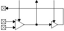
The IP2022 has an on-chip analog comparator which
uses alternate functions of the RG0, RG1, and RG2 port
pins. The RG1 and RG2 pins are the comparator negative
and positive inputs, respectively, while the RG0 pin is the
comparator output pin. To use the comparator, software
must program the port direction register (RGDIR) so that
RG1 and RG2 are inputs. RG0 may be set up as a
comparator output pin.
Figure 5-20 Analog Comparator
The comparator enable bits are cleared on reset, which
disables the comparator. To avoid drawing additional
current during power-down mode, the comparator should
be disabled before entering power-down mode. A 50 mV
hysteresis is applied between the inputs, when the
CMPHYS bit is set in the CMPCFG register.
5.8.1
CMPCFG Register
The CMPCFG register is used to enable the comparator,
to read the output of the comparator internally, to enable
the output of the comparator to the comparator output pin,
and to enable the hysteresis. Figure 5-21 shows the bits
in this register.
•
CMPEN—set to enable comparator, clear to disable.
•
CMPOE—set to enable the comparator output on the
RG0 pin, clear to disable.
•
CMPHYS—set to enable hysteresis, clear to disable.
•
CMPMOD—set for squelch or comparator mode for
Ethernet, clear for normal mode.
•
CMPRES—comparator result (read-only).
5.9
Linear Feedback Shift Register
Four linear feedback shift register (LFSR) units provide
hardware support for the computation-intensive inner
loops
of
algorithms
commonly
used
in
data
communications, such as:
•
Cyclic Redundancy Check (CRC)
•
Data Scrambling
•
Data Whitening
•
Encryption/Decryption
•
Hashing
The LFSR units implement a programmable architecture,
which can be adapted for algorithms used by the
Bluetooth, Ethernet, Homeplug, HomePNA, HomeRF,
IEEE 802.11, and USB communication protocols. Table 5-
14 shows the LFSR configurations used to support these
protocols. Figure 5-22 is a block diagram of the LFSR
architecture.
7
6
5
4
3
1
0
Reserved
Figure 5-21 CMPCFG Register
515-017.eps
+
-
CMPEN,
CMPHYS CMPRES CMPOE
RG2
RG0
RG1

