72
www.ubicom.com
IP2022 Data Sheet
5.7
Analog to Digital Converter (ADC)
The on-chip A/D converter has the following features:
•
10-bit ADC, ½ LSB accuracy
•
8 input channels
•
48 kHz maximum sampling rate
•
One-shot conversion.
•
Optional external reference voltage
•
Vmax = AVdd (max 2.7V)
•
Result returned in the ADCH and ADCL registers
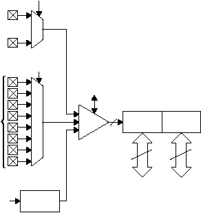
Figure 5-18 shows the A/D converter circuitry. The ADC
input pins use alternate functions of the Port G pins. The
result of an ADC sample is the analog value measured on
the selected pin. To correctly read an external voltage, the
pin being sampled must be configured as an input in the
port direction register (i.e. the RGDIR register). If the pin
is configured as an output, then the result will indicate the
voltage level being driven by the output buffer. The RG1
and RG2 port pins are also used as the analog
comparator input pins. The result of sampling the RG1 or
RG2 pins will be correct whether or not the comparator is
operating. The RG0 pin is also used as the comparator
output pin. If the comparator is enabled, then sampling the
RG0 pin will indicate the voltage level being driven by the
comparator. The RG3 pin is multiplexed with the external
reference voltage.
Figure 5-18 A/D Converter Block Diagram
5.7.1
ADC Reference Voltage
The reference voltage (Vref) can come from either the
RG3 port pin or from the AVdd supply voltage. If AVdd is
used, the RG3 port pin may be used as a channel of
analog input or as a general-purpose port pin.
Vref defines a voltage level which reads as one increment
of resolution below the full-scale voltage. The full-scale
voltage reads as 0x3FF, so the Vref voltage reads as
0x3FE and the A/D converter resolution is 10 bits. Table
5-12 shows the values reported at the upper and lower
limits of the ADC input voltage range.
5.7.2
ADC Result Justification
The 10 bits of the ADC value can be mapped to the 16 bits
of the ADCH/ADCL register pair in three different ways, as
shown in Table 5-13. In this table, the numbers in the cells
represent bit positions in the 10-bit ADC value, Z
represents zero (as opposed to bit position 0), and -9
represents the inversion of bit position 9.
515-016.eps
ADCH
A/D
Vref
Reference
Voltage
ADCREF
ADC Timer
8
7
0
ADCGO
10
ADCL
8
7
0
AVdd
RG7:0
System
Clock
ADCS2:0
RG3
Data Bus Data Bus
Table 5-12 ADC Values
Vin Voltage
ADC Value
0V
0x000
Vref/0x3FE
0x001
Vref
0x3FE
Vref + (Vref/0x3FE)
0x3FF
