52
www.ubicom.com
IP2022 Data Sheet
5.1.1
Port B Interrupts
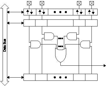
Figure 5-2 Port B Interrupt Logic
Any of the 8 Port B pins can be configured as an external
interrupt input. Logic on these inputs can be programmed
to sense rising or falling edges. When an edge is
detected, the interrupt flag for the port pin is set.
The recommended initialization sequence is:
1.
Configure the port pins used for interrupts as inputs
by programming the RBDIR register.
2.
Select the desired edge for triggering the interrupt
by programming the INTED register. This may set
interrupt flags. Be sure all enabled interrupt pins are
driven to valid logic levels, not floating.
3.
Clear the interrupt flags in the INTF register.
4.
Enable the interrupt input(s) by setting the corre-
sponding bit(s) in the INTE register.
5.
Set the GIE bit.
Figure 5-2 shows the Port B interrupt logic. Port B has
three registers for supporting external interrupts, the
INTED (Section 5.1.6), INTF (Section 5.1.7), and INTE
(Section 5.1.8) registers. The INTED register controls the
logic which selects the edge sensitivity (i.e. rising or falling
edge) of the Port B pins. When an edge of the selected
type occurs, the corresponding flag in the INTF register is
set, whether or not the interrupt is enabled. The interrupt
signal passed to the system interrupt logic is the OR
function of the AND of each interrupt flag in the INTF
register with its corresponding enable bit in the INTE
register.
5.1.2
Reading and Writing the Ports
The port registers are memory-mapped into the data
memory address space between 0x020 and 0x03A. In
addition, Port B has three extra registers located between
0x017 and 0x019 which are used to support external
interrupt inputs.
When two successive read-modify-write instructions read
and write the same I/O port with a very high clock rate, the
“write” part of one instruction might not occur soon enough
before the “read” part of the very next instruction, resulting
in the second instruction getting “old” data. To ensure
predictable results, avoid using two successive read-
modify-write instructions that access the same register if
the clock rate is high, or insert 2 nop instructions between
successive read-modify-write instructions (if the SYNC bit
in the FUSE1 register is clear, 3 nop instructions are
required). When reading from the RxOUT register rather
than the RxIN register, the CPU reads data from a register
instead of the port pins. In this case, the nop instructions
are not required.
5.1.3
RxIN Registers
The RxIN registers are virtual registers that provide read-
only access to the physical I/O pins. Reading these
registers returns the states on the pins, which may be
driven either by the IP2022 or an external device. If the
RB7
INTED Register
515-031.eps
RB6
RB1
RB0
INTF Register
INTE Register
Port B
Interrupt
