22
www.ubicom.com
IP2022 Data Sheet
The status register contains two bits to indicate the source
of the reset, WD and BO. The WD bit is cleared on reset
unless the reset was caused by the watchdog timer, in
which case the WD bit is set. The BO bit is cleared on
reset unless the reset was caused by the brown-out logic,
in which case, the BO bit is set.
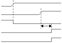
Figure 3-12 shows a power-up sequence in which RST is
not tied to the IOVDD pin and the IOVDD signal is allowed
to rise and stabilize before RST pin is brought high. The
device will actually come out of reset after the startup
stabilization period (Tstartup) from RST going high. The
WUDX2:0 bits of the FUSE0 register specify the length of
the stabilization period.
Figure 3-12 Power-On Reset, Separate RST Signal
The brown-out circuitry resets the chip when device
power (AVdd) dips below its minimum allowed value, but
not to zero, and then recovers to the normal value.
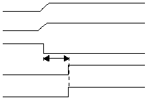
Figure 3-13 shows the on-chip Power-On Reset
sequence in which the RST and IOVDD pins are tied
together. The IOVDD signal is stable before the startup
timer expires. In this case, the CPU receives a reliable
reset.
Figure 3-13 Power-On Reset, RST Tied To IOVdd
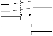
However, Figure 3-14 depicts a situation in which IOVDD
rises too slowly. In this scenario, the startup timer will time
out prior to IOVDD reaching a valid operating voltage level
(IOVDD min). This means the CPU will come out of reset
and start operating with the supply voltage below the level
required for reliable performance. In this situation, an
external RC circuit is recommended for driving RST. The
RC delay should exceed the time period required for
IOVDD to reach a valid operating voltage.
Figure 3-14 IOVdd Rise Time Exceeds Tstartup
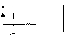
Figure 3-15 shows the recommended external reset
circuit. The external reset circuit is required only if the
IOVDD rise time has the possibility of being too slow.
Figure 3-15 External Reset Circuit
The diode D discharges the capacitor when IOVDD is
powered down.
R1 = 100
W
to 1K
W
will limit any current flowing into RST
from external capacitor C1. This protects the RST pin from
breakdown due to Electrostatic Discharge (ESD) or
Electrical Overstress (EOS).
R2 < 40K
W
is recommended to make sure that voltage
drop across R2 leaves the RST pin above a Vih level.
515-019.eps
IOVDD
RST
POR
Tstartup
Startup Timer3
(Time-Out)
Internal
Rest Signal
IOVDD
RST
POR
Tstartup
Startup Timer
(Time-Out)
Internal
Rest Signal
515-022.eps
IOVDD
RST
POR
Tstartup
Startup Timer
(Time-Out)
Internal
Rest Signal
515-020.eps
IOVDD
C1
R2
R1
515-021.eps
RST
IP2022


