IP2022 Data Sheet
www.ubicom.com
21
3.5.5
Disabled Resources
If a peripheral is disabled, it does not have the ability to set
an interrupt flag. The interrupt flag, however, is still a valid
source of interrupt.
If software sets an interrupt flag, the corresponding
interrupt enable bit is set, and the GIE bit is set, then the
CPU will be interrupted whether or not the peripheral is
enabled or disabled.
If a peripheral is disabled inside the ISR, then its interrupt
flag must be cleared to prevent a spurious interrupt from
being taken when the ISR completes.
3.5.6
Clock Stop Mode
When a speed change occurs, it is possible for the CPU
clock source to be disabled. The clock to the CPU core
may be disabled while the system clock is left running, or
the system clock may be disabled which also disables the
CPU core clock. When the system clock is disabled, the
interrupt logic continues to function, and the watchdog
timer and real-time timer may be enabled to keep running.
(For minimum power consumption in clock stop mode,
disable these timers if they are not needed.)
Recovery from clock stop mode to normal execution is
possible from these sources:
•
External interrupts (i.e. Port B interrupts)
•
Real-time timer interrupts
•
Watchdog timer overflow reset
•
Brown-out voltage reset
•
RST external reset
The first two sources listed above do not reset the chip, so
program execution continues from where it was stopped.
The last three sources reset the chip, so software must
perform all of its reset initialization tasks to recover. This
usually requires additional time, as compared to recovery
through an external interrupt.
3.6
Reset
There are five sources of reset:
•
Power-On Reset
•
Brown-Out Reset
•
Watchdog Reset
•
External Reset (from the RST pin)
•
Target Reset (from the debugging interface)
Each of these reset conditions causes the program
counter to branch to the top of the program memory (word
address 0xFFF0 or byte address 0x1FFE0).
The IP2022 incorporates a Power-On Reset (POR)
detector that generates an internal reset as DVdd rises
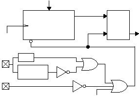
during power-up. Figure 3-11 is a block diagram of the
reset logic. It includes a 10-bit startup timer and a reset
latch. The startup timer controls the reset time-put delay.
The reset latch controls the internal reset signal. On
power-up, the reset latch is set (CPU held in reset), and
the startup timer starts counting once it detects a valid
logic high signal on the RST pin. Once the startup timer
reaches the end of the timeout period, the reset latch is
cleared, releasing the CPU from reset.
Figure 3-11 On-Chip Reset Circuit Block Diagram
10-Bit Asynchronous
Ripple Counter
(Start-Up
Timer)
R
S
Q
Brown-Out
Detection
RST
VDD
Watchdog Timer
Overflow
Internal
RC Clock
Time-Out
Internal
Reset Signal
(active low)
POR
Power-On Reset
515-023.eps
Clear
WUDX2:0
