10
www.ubicom.com
IP2022 Data Sheet
3.0
System Architecture
The IP2022 CPU executes from a 32K × 16 flash program
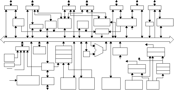
memory and an 8K × 16 RAM program memory. Figure 3-
1 shows the IP2022 detailed block diagram. The
maximum execution rate is 30 MIPS from flash and 100
MIPS from RAM. Speed-critical routines can be copied
from the flash memory to the RAM for faster execution.
The CPU operates on 8-bit data in 128 special-purpose
registers, 128 global registers, and 3840 bytes of data
memory. The special-purpose registers hold control and
status bits used for CPU control and for interface with
hardware peripherals (timers, I/O ports, A/D converter,
etc.).
Figure 3-1 IP2022 Detailed Block Diagram
RF7
60
I/O
8 mA
8 mA
I/O Port, Serial 2 RXD
RG0
61
AI/DO
4 mA*
4 mA*
Output Port, ADC0 Input, Comparator Output
RG1
62
AI/DO
4 mA*
4 mA*
Output Port, ADC1 Input, Comparator – Input
RG2
63
AI/DO
4 mA*
4 mA*
Output Port, ADC2 Input, Comparator + Input
RG3
64
AI/DO
4 mA*
4 mA*
Output Port, ADC3 Input, ADC reference Input
RG4
66
AI/DO
4 mA*
4 mA*
Output Port, ADC4 Input, SERDES1 Squelch – Input
RG5
67
AI/DO
4 mA*
4 mA*
Output Port, ADC5 Input, SERDES1 Squelch + Input
RG6
68
AI/DO
4 mA*
4 mA*
Output Port, ADC6 Input, SERDES2 Squelch – Input
RG7
69
AI/DO
4 mA*
4 mA*
Output Port, ADC7 Input, SERDES2 Squelch + Input
* GVDD = 2.5V
Table 2-1 Signal Descriptions (continued)
Name
Pin
Type
Sink
@ 3.3V
IOVDD
Source
@ 3.3V
IOVDD
Function
Internal Data Bus
Port A
RTCLK
SxCLK
Real-Time
Clock Driver
OSC
Driver
Timer 1
(T1)
Port E
Port F
Port G
(2) Serializer/
Deserializers
Analog
Comparator
Timer 2
(T2)
Port B
Timer 0
(T0)
Interrupt
Port D
Port C
Edge Det.
Parallel
Slave
Peripheral
ADC
Multiplexer
Divider
CPU Core Clock
Multiplexer
Divider
PLL
Divider
Divider
4KB Data
Memory
515-038.eps
System
Clock
Real-Time
Timer
Reset
W
ALU
Watchdog Timer
with Pre-Scaler
ISD
Writeback
ISP
Brown
Out
POR
RST
Execute
Decode
64KB Flash
Program
Memory
16KB RAM
Program
Memory
Fetch
Internal
RC
Clock
(4) LFSR
Units
Ext. Memory
Interface
