IP2022 User’s Manual—System Architecture
www.ubicom.com
47
timeout period, the reset latch is cleared, releasing the CPU from
reset.
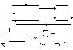
Figure 2-7 On-Chip Reset Circuit Block Diagram
The status register contains two bits to indicate the source of the
reset, WD and BO. The WD bit is cleared on reset unless the reset
was caused by the watchdog timer, in which case the WD bit is set.
The BO bit is cleared on reset unless the reset was caused by the
brown-out logic, in which case, the BO bit is set.
10-Bit Asynchronous
Ripple Counter
(Start-Up
Timer)
R
S
Q
Brown-Out
Detection
RST
VDD
Watchdog Timer
Overflow
Internal
RC Clock
Time-Out
Internal
Reset Signal
(active low)
POR
Power-On Reset
515-023.eps
Clear
WUDX2:0
