Peripherals—IP2022 User’s Manual
324
www.ubicom.com
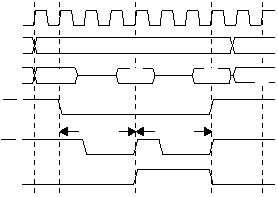
A read cycle to external memory has the timing shown in Figure 4-
20. Write cycle timing is shown in Figure 4-21. All external memory
cycles are 16-bit transfers, with the low byte (A0 = 0) followed by
the high byte (A0 = 1).
Figure 4-20 Read Cycle
Table 4-16 SRAM Access Time Specification
CPU Core Clock Frequency (MHz) SRAM Access Time (ns)
80
35
100
25
120
25
150
12/15/20*
* Depends on minimum WR pulse width specification.
RC7:0
RD7:0
LE
Clock
515-088.eps
RD
A0
ADDRH
ADDRL
DATAH
DATAL
ADDRH
ADDRL
Taccess
Taccess
