Peripherals—IP2022 User’s Manual
306
www.ubicom.com
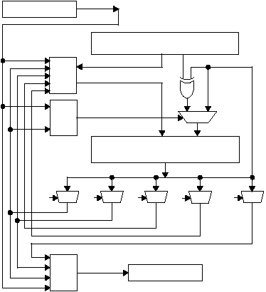
Figure 4-15 LFSR Block Diagram
The 40-bit residue register and its surrounding circuits are the
computational core of an LFSR unit. On every clock cycle, 39
output bits from the register are available at the input for
performing a shift operation or a polynomial add/subtract-and-shift
operation. Four 40-bit multiplexers at the output of the residue
Polynomial Register (POLYx)
Residue Register (RESx)
1..39
1..39
0..39
0
0
0
1
0..38
0..39
FB1
0..39
FB2
0..39
FB3
0..39
DOUT
D0
Source
Gating
POLY
Source
Gating
DOUT
Source
Gating
DATAOUT Register
DATAIN Register
515-082.eps
D0
POLY_XOR_EN
DOUT
DIN
0..39
FB4
