IP2022 User’s Manual—Peripherals
www.ubicom.com
295
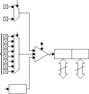
Figure 4-13 Analog-to-Digital Converter Block Diagram
The RG1 and RG2 port pins are also used as the analog
comparator input pins. The result of sampling the RG1 or RG2
pins will be correct whether or not the comparator is operating.
The RG0 pin is also used as the comparator output pin. If the
comparator is enabled, then sampling the RG0 pin will indicate the
voltage level being driven by the comparator. The RG3 pin is
multiplexed with the external reference voltage.
515-016.eps
ADCH
A/D
Vref
Reference
Voltage
ADCREF
ADC Timer
8
7
0
ADCGO
10
ADCL
8
7
0
AVdd
RG7:0
System
Clock
ADCS2:0
RG3
Data Bus Data Bus
