Peripherals—IP2022 User’s Manual
250
www.ubicom.com
I/O port pins. The port direction register has priority over the timer
configuration, so the port direction register must be programmed
appropriately for each of these four signals if their associated timer
functions are used. Each timer should be enabled before its
interrupt is enabled.
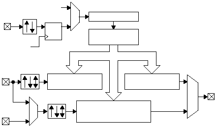
Figure 4-5 is a block diagram showing the registers and I/O pins
of one timer. Each timer is based on a 16-bit counter/timer driven
by a 15-bit prescaler. The input of the prescaler can be either the
system clock or an external clock signal which is internally
synchronized to the system clock. The counter cannot be directly
written by software, but it may be cleared by writing to the TxRST
bit in the TxCTRL register.
Figure 4-5 Multi-Function Timer Block Diagram
515-005.eps
TxCPI1
TxCAP1H/TxCAP1L
Register
TxOUT
TxCMP1H/TxCMP1L
Register
TxCLK
D Q
TxCPI2
TxCAP2H/TxCAP2L
or TxCMP2H/TxCMP2L
Register
TxCNTH/TxCNTL
Register
15-Bit Prescaler
System
Clock
System
Clock
