© 2005 Ubicom, Inc. All rights reserved.
- 31 -
www.ubicom.com
SX20AC/SX28AC
15.4 RAM Addressing
Direct Addressing
The FSR register must initialized with an appropriate
value in order to address the desired RAM register. The
following table and code example show how to directly
access the banked registers.
Indirect Addressing
To access any register via indirect addressing, simply
move the eight-bit address of the desired register into the
FSR and use INDF as the operand. The example below
shows how to clear all RAM locations from 10h to 1Fh in
all eight banks:
15.5 The Bank Instruction
Often it is desirable to set the bank select bits of the FSR
register in one instruction cycle. The Bank instruction
provides this capability. This instruction sets the upper
bits of the FSR to point to a specific RAM bank without
affecting the other FSR bits.
Example:
15.6 Bit Manipulation
The instruction set contains instructions to set, reset, and
test individual bits in data memory. The device is capable
of bit addressing anywhere in data memory.
15.7 Input/Output Operation
The device contains three registers associated with each
I/O port. The first register (Data Direction Register), con-
figures each port pin as a Hi-Z input or output. The sec-
ond register (TTL/CMOS Register), selects the desired
input level for the input. The third register (Pull-Up Regis-
ter), enables a weak pull-up resistor on the pin configured
as a input. In addition to using the associated port regis-
ters, appropriate values must be written into the MODE
register to configure the I/O ports.
When two successive read-modify-write instructions are
used on the same I/O port with a very high clock rate, the
"write" part of one instruction might not occur soon
enough before the "read" part of the very next instruction,
resulting in getting "old" data for the second instruction.
To ensure predictable results, avoid using two successive
read-modify-write instructions that access the same port
data register if the clock rate is high.
15.8 Increment/Decrement
The bank of 31 registers serves as a set of accumulators.
The instruction set contains instructions to increment and
decrement the register file. The device also includes both
INCSZ fr (increment file register and skip if zero) and
DECSZ fr (decrement file register and skip if zero)
instructions.
15.9 Loop Counting and Data Pointing
Testing
The device has specific instructions to facilitate loop
counting. The DECSZ fr (decrement file register and skip
if zero) tests any one of the file registers and skips the
next instruction (which can be a branch back to loop) if
the result is zero.
15.10 Branch and Loop Call Instructions
The device contains an 8-level hardware stack where the
return address is stored with a subroutine call. Multiple
stack levels allow subroutine nesting. The instruction set
supports absolute address branching.
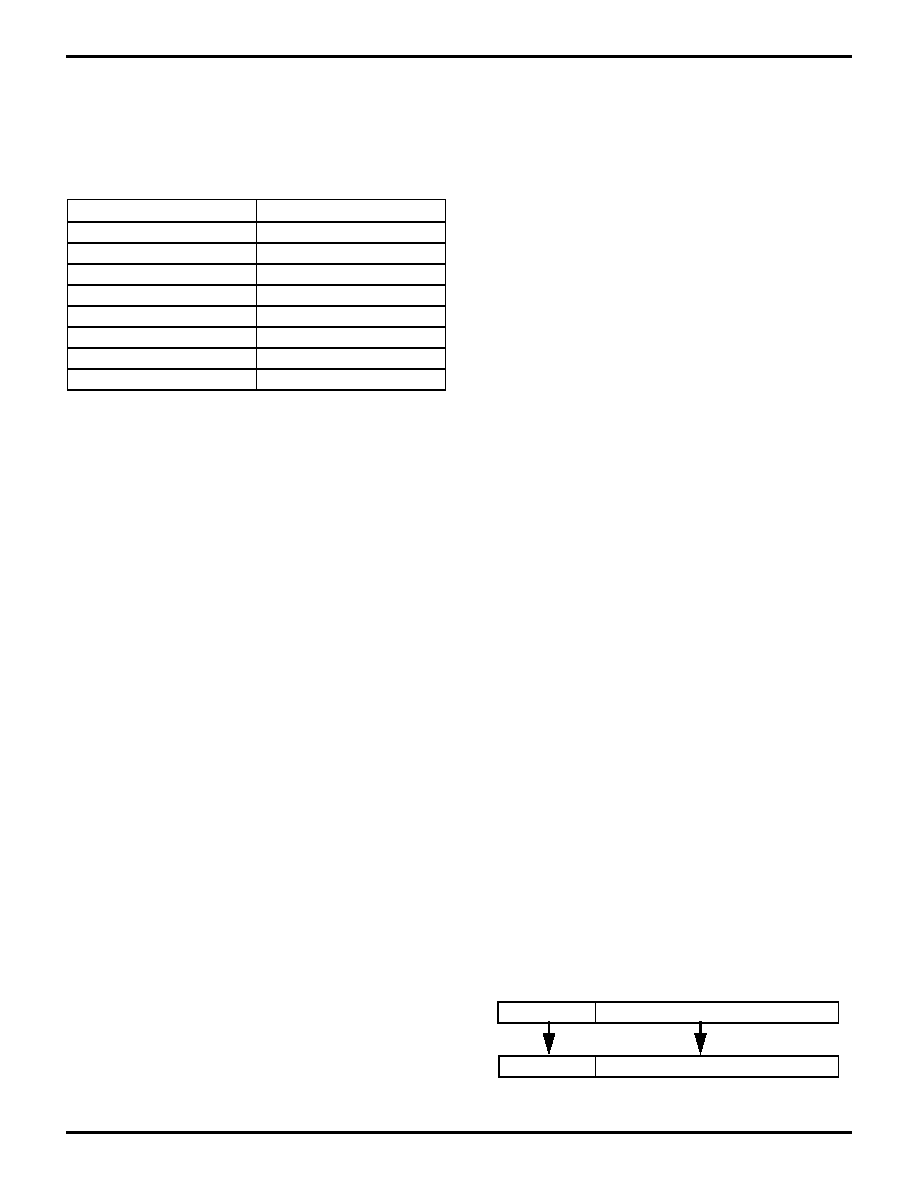
15.10.1 Jump Operation
When a JMP instruction is executed, the lower nine bits
of the program counter is loaded with the address of the
specified label. The upper two bits of the program
counter are loaded with the page select bits, PA1:PA0,
contained in the STATUS register. Therefore, care must
be exercised to ensure the page select bits are pointing
to the correct page before the jump occurs.
Bank
FSR Value
0
010h
1
030h
2
050h
3
070h
4
090h
5
0B0h
6
0D0h
7
0F0h
mov
FSR,#$070
;Select RAM Bank 3
clr
$010
;Clear register 10h on
;Bank 3
mov
FSR,#$D0
;Select RAM Bank 6
clr
$010
;Clear register 10h on
;Bank 6
clr
FSR
;clear FSR to 00h (at address
;04h)
:loop
setb SFR.4
;set bit 4: address 10h-1Fh,
;30-3Fh, etc
clr
INDF
;clear register pointed to by
;FSR
incsz FSR
;increment FSR and test, skip
;jmp if 00h
jmp
:loop
;jump back and clear next
;register
bank $F0
;Select Bank 7 in FSR
inc
$1F
;increment file register
;1Fh in Bank 7
STATUS<6:5>
JMP LABEL
PC<10:9>
PC<8:0>
