© 2005 Ubicom, Inc. All rights reserved.
- 16 -
www.ubicom.com
SX20AC/SX28AC
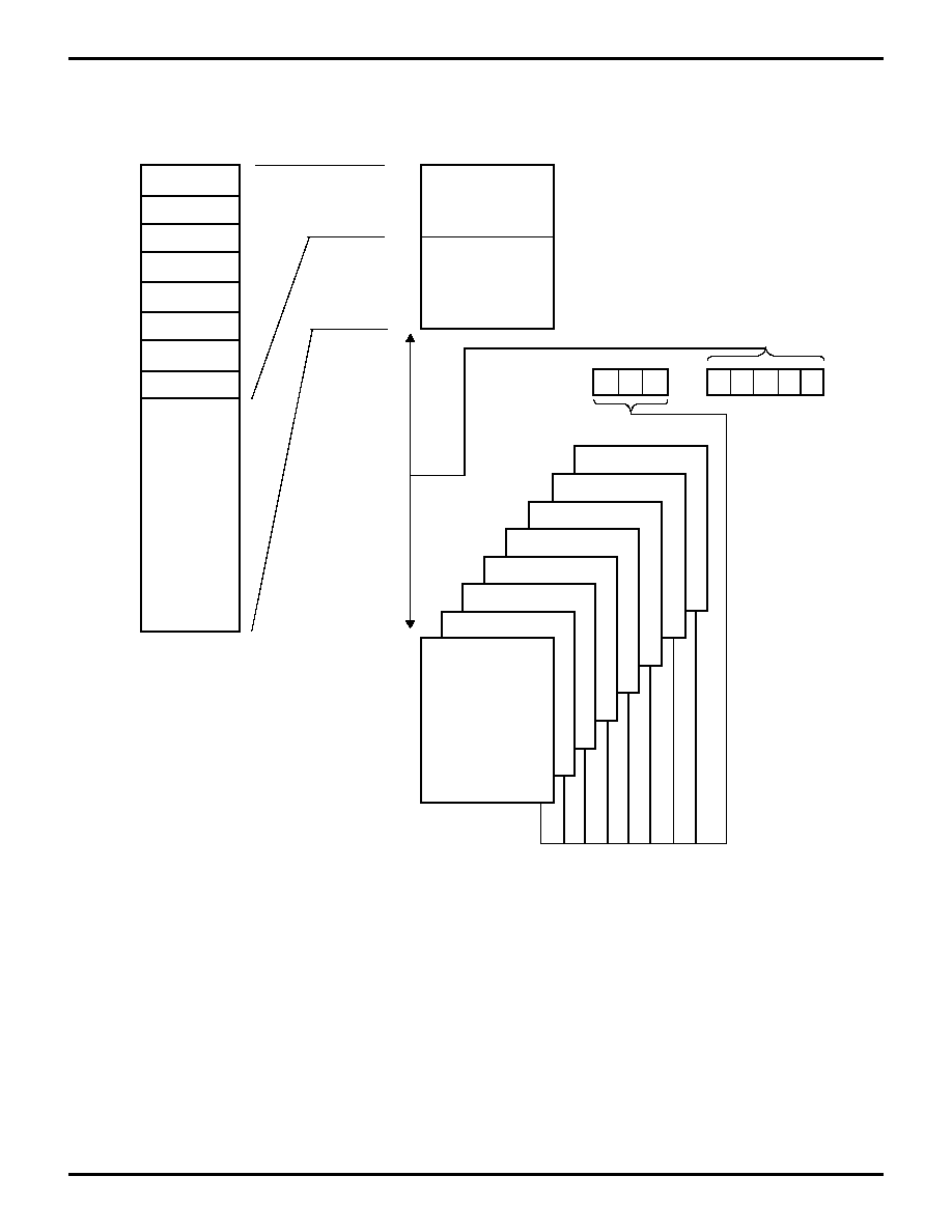
Figure 6-1. Data Memory Organization
Function Registers and Global Registers
INDF
RTCC
PC
STATUS
FSR
RA
RB
RC
Global
Bank 7
Bank 6
Bank 5
Bank 4
Bank 3
Bank 2
Bank 1
Bank 0
30
50
70
90
B0
D0
F0
3F
5F
7F
9F
BF
DF
FF
00
0
00
1
01
0
01
1
10
0
10
1
11
0
11
1
00
07
0F
10
1F
FSR bits
SRAM
(16 bytes
each bank
128 bytes
total)
7
6
5
4 3
2 1 0
Bank 0 is always accessed for
the lower 16 addresses,
irrespective of the three high-
order bits of FSR.
Registers
(8 bytes)
Bank 0
SRAM
(8 bytes)
08
Direct
Registers
00
01
02
03
04
05
06
07
08
09
0A
0B
0C
0D
0E
0F
10
1F
Instruction Opcode bits

