1
2
3
4
5
6
7
8
9
10
11
12
NexFlash Technologies, Inc.
3
PRELIMINARY
NXSF011C-0599
05/25/99 ©
NX26F080A
NX26F160
....
....
NX26F080A or
NX26F160
U0
NX26F080A or
NX26F160
U8
NX26F080A or
NX26F160
U9
NX26F080A or
NX26F160
U10
NX26F080A or
NX26F160
U11
NX26F080A or
NX26F160
U1
NX26F080A or
NX26F160
U2
NX26F080A or
NX26F160
U3
SCK
SIO
MICROCONTROLLER / MICROPROCESSOR
DSP or ASIC
0
A0
0
A1
0
A2
1
A3
1
A0
0
A1
0
A2
1
A3
0
A0
1
A1
0
A2
1
A3
1
A0
1
A1
0
A2
1
A3
1
A0
1
A1
0
A2
0
A3
0
A0
1
A1
0
A2
0
A3
1
A0
0
A1
0
A2
0
A3
0
A0
0
A1
0
A2
0
A3
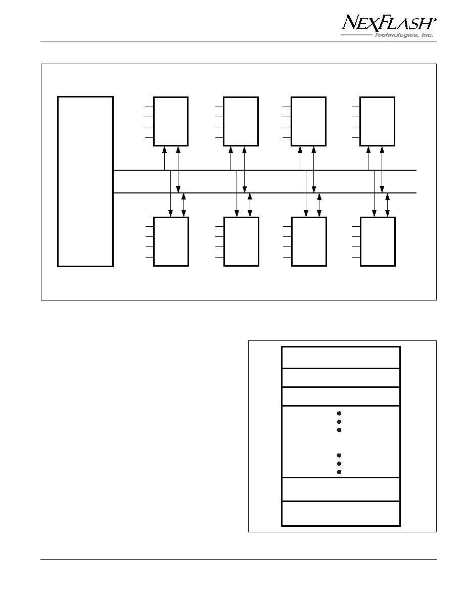
Figure 2. NX26F080A or NX26F160 Used in a Multi-device Configuration with up to 16-Devices on the 2-wire NSX
FUNCTIONAL OVERVIEW
The
NexFlash NX26F080A and NX26F160 provide up to
8M-bits or 16M-bits of non-volatile memory organized as
2,048 or 4,096 small sectors of 536 bytes (4,288 bits) each
(Figure 3). Each sector is individually addressable using
basic instruction sequences and control functions commu-
nicated through the devices 2-wire NXS interface.
Read and Erase/Write Instruction Sequences
The NX26F080A and NX26F160 have two basic instruction
sequences: Read and Erase/Write. Unlike some other
Flash technologies, the erase and write operations of the
NX26F080A and NX26F160 are performed together in one
single operation (as fast as 5 ms per sector). Thus,
pre-erase of the memory is not necessary.
Both Read and Erase/Write instructions are made up of a
series of serial bit fields that include command, sector
address, device address, and sector data. The Read
instruction sequence also allows the device to be polled for
Ready/Busy status.
Sector 0 (0000H)
4288 Bits (536 Bytes) Per Sector
Sector 1 (0001H)
Sector 2 (0002H)
Sectors 3-2045/4093
(0003-07FD/0FFDH)
Sector 2046/4094 (07FE/0FFEH)
Sector 2047/4095 (07FF/0FFFH)
Figure 3.
NexFlash's NX26F080A and NX26F160 Array
