The In-Circuit Debugger Survial Guide

1F00  1170          bcf    0x70,0x2
1F01  1903          btfsc  STATUS,ZERO
1F02  1570          bsf    0x70,0x2    ; Copy Zero Bit
1F03  1370          bcf    0x70,0x6
1F04  1B03          btfsc  STATUS,RP1
1F05  1770          bsf    0x70,0x6    ; Copy RP1 Bit
1F06  12F0          bcf    0x70,0x5
1F07  1A83          btfsc  STATUS,RP0
1F08  16F0          bsf    0x70,0x5    ; Copy RP0 Bit

1F09  1703          bsf    STATUS,RP1
1F0A  1683          bsf    STATUS,RP0  ; Select Bank 3

1F0B  00ED          movwf  0x6D        ; Copy Working Register to 0x6D

1F0C  3064          movlw  0x64
1F0D  05F0          andwf  0x70   	; Clear Bits we have not worried about yet
					; !(RP1, RP2 & Zero)

1F0E  0803          movf   STATUS,W
1F0F  399B          andlw  0x9B    	; Exclude Bits we have already read (RP1, RP2 & Zero)

1F10  04F0          iorwf  0x70         ; Or Result together (XOR?)

1F11  0804          movf   FSR,W 	; Indirect Data Memory Address Pointer
1F12  00EE          movwf  0x6E         ; Store Temporarly at 0x6E

1F13  080A          movf   PCLATH,W     ; Store Temporarly at 0x6F
1F14  00EF          movwf  0x6F

1F15  301F          movlw  0x1F
1F16  008A          movwf  PCLATH       ; Set Upper Location

1F17  080E          movf   0xE,W	; Reserved
1F18  00EB          movwf  0x6B         ; Store Temporarly a 0x6B

1F19  1703          bsf    STATUS,RP1
1F1A  1683          bsf    STATUS,RP0	; Select Bank 3

1F1B  30E0          movlw  0xE0         ; 0x60
1F1C  05EC          andwf  0x6C

1F1D  1706          bsf    TRISB,0x6	; Set Clock Input
1F1E  1386          bcf    TRISB,0x7    ; Set Data  Output
1F1F  1283          bcf    STATUS,RP0   ; Select Bank 2
1F20  1386          bcf    PORTB,0x7	; Clear Data
1F21  1683          bsf    STATUS,RP0	; Select Bank 3

1F22  0AEC  Loop    incf   0x6C         ;
1F23  1D6C          btfss  0x6C,0x2     ; Skip if Set
1F24  2F22          goto   0x1F22 (Loop); loop until bit 2 is set
1F25  116C          bcf    0x6C,0x2     ; Clear Bit 2

1F26  1283          bcf    STATUS,RP0   ; Select Bank 2 -> Access to Ports

1F27  0064  HitoLo  clrwdt
1F28  1B06          btfsc  PORTB,0x6(CLOCK) ; Loop until High to Low Transition
1F29  2F27          goto   0x1F27 (HitoLo)

1F2A  0064  LotoHi  clrwdt
1F2B  1F06          btfss  PORTB,0x6(CLOCK) ; Loop until low to high Transition
1F2C  2F2A          goto   0x1F2A (LotoHi)

1F2D  1786          bsf    PORTB,0x7 (DATA) ; Set Data Bit High

1F2E  1683          bsf    STATUS,RP0 	; Select BANK 3 -> Access to Debug Registers

1F2F  0AEC          incf   0x6C
1F30  1DEC          btfss  0x6C,0x3
1F31  2F2F          goto   0x1F2F
1F32  11EC          bcf    0x6C,0x3 	; Clear Bit 3

1F33  1283          bcf    STATUS,RP0   ; Select BANK 2 -> Access to Ports
1F34  1386          bcf    PORTB,0x7 (DATA) ; Clear Data

1F35  0064          clrwdt
1F36  1B06          btfsc  PORTB,0x6 (CLOCK) ; Loop until High to Low Transition
1F37  2F35          goto   0x1F35

1F38  0064          clrwdt
1F39  1F06          btfss  PORTB,0x6 (CLOCK) ; Loop until low to high Transition
1F3A  2F38          goto   0x1F38


1F3B  1003          bcf    STATUS,CARRY      ; Clear Carry
1F3C  1683          bsf    STATUS,RP0        ; Select BANK 3 -> Access to Debug Registers
1F3D  1BEC          btfsc  0x6C,0x7          ; Copy Bit 7 of 6C
1F3E  1403          bsf    STATUS,CARRY
1F3F  1283          bcf    STATUS,RP0        ; Select BANK 2 -> Access to Ports

1F40  1386          bcf    PORTB,0x7 (DATA)  ; Clear Data
1F41  1C03          btfss  STATUS,CARRY      ; Copy Bit 7 to Data
1F42  1786          bsf    PORTB,0x7 (DATA)

1F43  1B06          btfsc  PORTB,0x6 (CLOCK) ; Loop until High to Low Transition
1F44  2F43          goto   0x1F43


1F45  1683          bsf    STATUS,RP0        ; Select BANK 3 -> Access to Debug Registers
1F46  1786          bsf    TRISB,0x7 (DATA)  ; Make DATA Input
1F47  0064          clrwdt

1F48  0AEC          incf   0x6C

1F49  1283          bcf    STATUS,RP0        ; Select BANK 2 -> Access to Ports
1F4A  1003          bcf    STATUS,CARRY
1F4B  1B86          btfsc  PORTB,0x7 (DATA)  ; Read Data
1F4C  1403          bsf    STATUS,CARRY
1F4D  1683          bsf    STATUS,RP0        ; Select BANK 3 -> Access to Debug Registers
1F4E  13EC          bcf    0x6C,0x7          ; Store 6C
1F4F  1803          btfsc  STATUS,CARRY
1F50  17EC          bsf    0x6C,0x7


1F51  1283  loop    bcf    STATUS,RP0        ; Select BANK 2 -> Access to Ports

1F52  0064          clrwdt
1F53  1F06          btfss  PORTB,0x6 (CLOCK) ; Loop until low to high Transition
1F54  2F52          goto   0x1F52

1F55  1386          bcf    PORTB,0x7 (DATA)
1F56  1683          bsf    STATUS,RP0        ; Select BANK 3 -> Access to Debug Registers
1F57  1386          bcf    PORTB,0x7 (DATA)
1F58  1003          bcf    STATUS,CARRY
1F59  1B6B          btfsc  0x6B,0x6
1F5A  1403          bsf    STATUS,CARRY
1F5B  1283          bcf    STATUS,RP0        ; Select BANK 2 -> Access to Ports
1F5C  1386          bcf    PORTB,0x7 (DATA)
1F5D  1803          btfsc  STATUS,CARRY
1F5E  1786          bsf    PORTB,0x7 (DATA)

1F5F  0064          clrwdt
1F60  1B06          btfsc  PORTB,0x6 (CLOCK) ; Loop until High to Low Transition
1F61  2F5F          goto   0x1F5F

1F62  1683          bsf    STATUS,RP0        ; Select BANK 3 -> Access to Debug Registers
1F63  1786          bsf    TRISB,0x7 (DATA)  ; Make Data an Input!
1F64  1003          bcf    STATUS,CARRY
1F65  0D8F          rlf    0x0F
1F66  0DEB          rlf    0x6B
1F67  0AEC          incf   0x6C
1F68  1283          bcf    STATUS,RP0        ; Select BANK 2 -> Access to Ports
1F69  1003          bcf    STATUS,CARRY
1F6A  1B86          btfsc  PORTB,0x7 (DATA)  ; read data
1F6B  1403          bsf    STATUS,CARRY
1F6C  1683          bsf    STATUS,RP0        ; Select BANK 3 -> Access to Debug Registers
1F6D  1803          btfsc  STATUS,CARRY

1F6E  140F          bsf    0xF,0x0            (Reserved)

1F6F  1E6C          btfss  0x6C,0x4
1F70  2F51          goto   0x1F51

1F71  1FEC          btfss  0x6C,0x7
1F72  2F84          goto   0x1F84


1F73  086B          movf   0x6B,W	     ; Restore Registers
1F74  008E          movwf  0xE (Reserved)
1F75  086F          movf   0x6F,W
1F76  008A          movwf  PCLATH
1F77  086E          movf   0x6E,W
1F78  0084          movwf  FSR
1F79  0870          movf   0x70,W
1F7A  0083          movwf  STATUS


1F7B  1683          bsf    STATUS,RP0
1F7C  1703          bsf    STATUS,RP1	     ; BANK SELECT 3

1F7D  0EED          swapf  0x6D
1F7E  0E6D          swapf  0x6D,W
1F7F  1F70          btfss  0x70,0x6
1F80  1303          bcf    STATUS,RP1
1F81  1EF0          btfss  0x70,0x5
1F82  1283          bcf    STATUS,RP0

1F83  0008          return  		      ; Pop of stack?


1F84  0E6B          swapf  0x6B,W
1F85  3907          andlw  0x7 		      ; 8 Possible Combinations of High Nibble
1F86  0782          addwf  PCL
1F87  2FAE          goto   0x1FAE
1F88  2FB2          goto   0x1FB2
1F89  2FB0          goto   0x1FB0
1F8A  2FB4          goto   0x1FB4
1F8B  2F9A          goto   0x1F9A
1F8C  2FA6          goto   0x1FA6
1F8D  2F8F          goto   0x1F8F
1F8E  2FA1          goto   0x1FA1

1F8F  086B          movf   0x6B,W
1F90  3907          andlw  0x7                ; 8 Possible Combinations of Low Nibble
1F91  0782          addwf  PCL
1F92  2FB6          goto   0x1FB6
1F93  2FBC          goto   0x1FBC
1F94  2FB9          goto   0x1FB9
1F95  2FBF          goto   0x1FBF
1F96  2FC2          goto   0x1FC2
1F97  2FCE          goto   0x1FCE
1F98  2FA1          goto   0x1FA1
1F99  2FA1          goto   0x1FA1


1F9A  1383          bcf    STATUS,IRP ; (Bank 0,1 00h ffh) Used for Indirect Addressing
1F9B  186B          btfsc  0x6B,0x0
1F9C  1783          bsf    STATUS,IRP ; (Bank 2,3 100 1ffh)

1F9D  080F          movf   0xF,W
1F9E  0084          movwf  0x4

1F9F  0800          movf   0x0,W


1FA0  008F          movwf  0xF          ; High Byte

** WAIT FOR HIGH TO LOW TRANSITION ON DATA

1FA1  1283          bcf    STATUS,RP0	; Bank 2
1FA2  0064          clrwdt
1FA3  1F06          btfss  PORTB,DATA	; Read Data Line
1FA4  2FA2          goto   0x1FA2       ; Wait for low to High Transition

1FA5  2F19          goto   0x1F19


** SAVE VALUE of 0x6D to FILE REGISTERS (0x0F)

1FA6  1383          bcf    STATUS,IRP   ; Indirect Addressing Register Bank
1FA7  186B          btfsc  0x6B,0x0     ; If 6B Bit 0 = 0 Bank 0,1 (00h  -> FFh)
1FA8  1783          bsf    STATUS,IRP   ;             = 1 Bank 2,3 (100h -> 1FFh)

1FA9  080F          movf   0xF,W        ;
1FAA  0084          movwf  FSR		; Move Address of Data Memory from W to FSR
1FAB  086D          movf   0x6D,W       ;
1FAC  0080          movwf  0x0          ; Save Contents of REG6D to Addr 0xF
1FAD  2FA1          goto   0x1FA1

** SEND VALUE IN 6D

1FAE  086D          movf   0x6D,W
1FAF  2FA0          goto   0x1FA0

** SEND VALUE IN 6E

1FB0  086E          movf   0x6E,W
1FB1  2FA0          goto   0x1FA0

** SEND VALUE IN 70

1FB2  0870          movf   0x70,W
1FB3  2FA0          goto   0x1FA0

** SEND VALUE IN 6F

1FB4  086F          movf   0x6F,W
1FB5  2FA0          goto   0x1FA0


1FB6  080F          movf   0xF,W
1FB7  00ED          movwf  0x6D
1FB8  2FA1          goto   0x1FA1

1FB9  080F          movf   0xF,W
1FBA  00EE          movwf  0x6E
1FBB  2FA1          goto   0x1FA1

1FBC  080F          movf   0xF,W
1FBD  00F0          movwf  0x70
1FBE  2FA1          goto   0x1FA1


1FBF  090F          comf   0xF,W
1FC0  00EF          movwf  0x6F
1FC1  2FA1          goto   0x1FA1

1FC2  080F          movf   0xF,W
1FC3  1283          bcf    STATUS,RP0   ; Bank 0?
1FC4  008C          movwf  0xC          ; PIR1
1FC5  1683          bsf    STATUS,RP0	; Bank 1
1FC6  138C          bcf    0xC,0x7 	; PIE1
1FC7  150C          bsf    0xC,0x2      ; PIE1

1FC8  3055          movlw  0x55
1FC9  008D          movwf  0xD		; PIE2

1FCA  30AA          movlw  0xAA
1FCB  008D          movwf  0xD		; PIE2

1FCC  148C          bsf    0xC,0x1
1FCD  2FA1          goto   0x1FA1


1FCE  080F          movf   0xF,W	; TMR1H
1FCF  1283          bcf    STATUS,RP0	; BANK0
1FD0  008D          movwf  0xD          ; PIR2
1FD1  1683          bsf    STATUS,RP0   ; BANK1
1FD2  138C          bcf    0xC,0x7        (PIE1)
1FD3  140C          bsf    0xC,0x0        (
1FD4  1283          bcf    STATUS,RP0
1FD5  080C          movf   0xC,W
1FD6  1683          bsf    STATUS,RP0
1FD7  2FA0          goto   0x1FA0
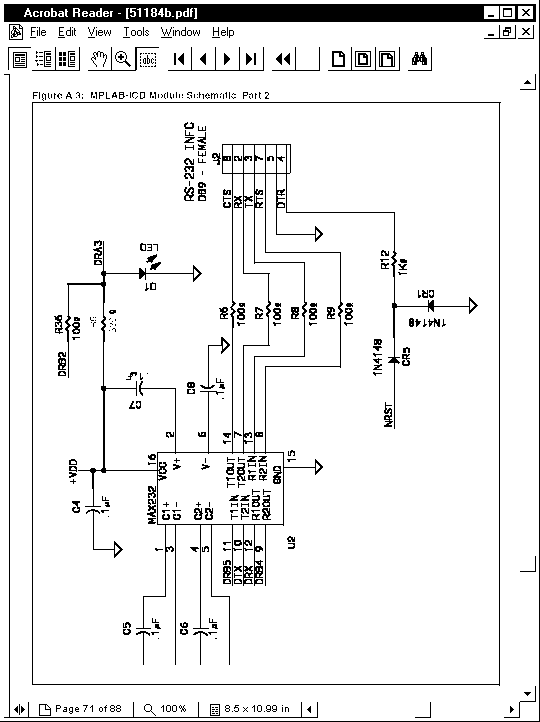
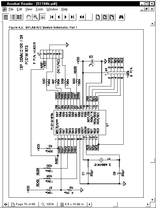
The ICD module itself has a 3,6864 Mhz Xtal.
The demo board has an empty socket and link for (optional) osc module, but normally runs as an RC osc...
Let me direct you to an article which John Day, A Principal Field Application Engineer for Microchip wrote in Circuit Cellar, Issue 109, August 1999.
John writes, "The debug kernel is downloaded along with the target firmware via the ICSP interface. A non-maskable interrupt vectors execution to the kernel when the program counter equals a preselected hardware breakpoint address, after a single step, or when a halt command is received from the host."
"As with all interrupts, this interrupt pushes the return address onto the stack. On reset, the breakpoint register is set equal to the reset vector, so the kernel is entered immediately when the device comes out of reset. The ICD module issues a reset to the target '16F877 immediately after a download, the kernel is entered and control is passed to MPLAB running on the host."
"You can then command the target processor as you choose. All RAM registers including the PC and other special function registers can be modified or interrogated. You can single step, set a breakpoint, animate and start or stop full speed execution."
Now it doesn't take too much effort to work out that we need two bytes for the Breakpoint Register. An considering the 16F87x documentation shows only to registers which are reserved, life couldn't be easier. Locations 0x18E and 0x18F are the breakpoint register. I've written a little program which allows me to access internal registers via the serial port. This is great for debugging/learning the operation of peripherals. What this has also told me, that in normal operation these two registers can't be written too.
So when a breakpoint occurs where does the program vector too? Maybe 0x1F00, the start of that all secret debug target code?
Tonight's Homework: Write a program at 0x1F00 to flash a LED or something similar. Then write a loop at 0x0000 so in normal operation, the code at 0x1F00 never gets executed. Then run the program both with the Debug Bit Clear and Set. Then summarize your observations to the PIC List . . . . (No I won't be marking it)
I have done this a couple of months back, but where getting mixed results. This was at the time my programmer was also given mixed results!, thus I could never verify exactly what was happening. However I suspect there is more to this. I also observed that is I placed about 10 NOP's at 0000 it would work. We do know for sure, reading from the ICD manual that you need to program the first location with a NOP. This is due to the fact that the breakpoint register is compared to the PC address after execution of the instruction.
John continues to write under the heading Silicon Requirements, "The breakpoint address register and compactor, along with some logic to single step and recognize asynchronous commands from the host, make up most of what is needed in the silicon. The ICSP interface is in place to support programming and doesn't constitute and additional silicon requirement."
"recognize asynchronous commands" This has stumped me. What I believe is that there is some other ICSP command which enables and disables operation? I'm open to any suggestions . . . .
Also check my reply to Robin Abbott dated Mon, 24 Jan 2000 if you are desperately scratching for more information. . . http://www.infosite.com/%7Ejkeyzer/piclist/2000/Jan/1552.html
From MChip App Note TB033:
Certain resources are consumed when the MPLAB™-ICD In-Circuit Debugger is used to develop code. These resources are released when the debugger is not used. The resources include:
- Last 256 words of program memory: IF00h to IFFh
- Program memory location 0000h must be a NOP instruction
- Pins RB6 and RB7: CLK and Data for ICD
- MCLR/VPP used for programming @ 13V
- Data memory locations 70h, 1EBh – 1EFh (Eh? its 18Eh - 18Fh right?)
Processor File Registers Used Program Memory Used PIC16F870/871/872 0x70, 0x0BB-0x0BF 0x06E0-0x07FF PIC16F873/874 0x70, 0x0EB-0x0F0 0x0EE0-0x0FFF PIC16F876/877 0x70, 0x1EB-0x1EF 0x1F00-0x1FFF- 1 Level of stack