This is a mouthful, but ...
How do you program a PIC to be a programming device without a programmer, and why would you want to build a programmer if you already have one that can program the PIC to be a programmer.
The answer here is to try to build a very cheap circuit that is easy to build and does not need any special software to do the job. That way, after it has done it's job, the parts can end up back into the junk box. The simplest approach I could come up with, was to use a simple circuit, the PC Serial Port and be able to program a PIC just by sending (2) different ASCII codes. This way, you do not need any special software to set up, and the circuit can be built out of junk bits and pieces. This programmer is not capable of reading data from a PIC, but for the purpose it is meant for, that doesn't matter.
Two things we need to extract out of the serial data are :-
(1) Clock pulses
(2) Data bits
While programming, new data bits entering the PIC are placed on pin RB7 while the clock pulse appearing on pin RB6 is in a high state. The PIC will accept the new data when the clock line is brought low. Programming comands are 6 bits long, and the data that follows consists of a Low Start Bit plus 14 data bits that the PIC will store in memory and then a Low Stop Bit. The circuit shown below extracts clock pulses and data bits from the data stream produced by sending the (2) ASCII codes from the serial port.
The ASCII characters that produce this data are :-
#0
Null Character
#127
DEL Character
Circuit Diagram

The circuit is very simple and is also easy to construct. ASCII data comes on the Tx line from the PC serial port on Pin 3 of a DB9 connector. This data is shown in MAGENTA and can be around 11 volts above and below ground. This is damaging to a circuit that is designed to run on 5 volts, so R1 and Z1 reduce the positive voltage to 5 volts and the negative voltage is blocked by D1.
Next the data bits that the PIC will store are extracted from the ASCII value. The circuit path for this is in TEAL.
Now the tricky part...
The IC used in the circuit is a Schmitt Trigger Quad NAND gate. U1a is configured as a monostable multivibrator. When the incoming signal goes from 0V to 5V, capacitor C1 charges via R3. This has the effect of producing a very short +ve pulse at U1a pin 2. U1a pin 1 is tied to the 5 volt rail so the output of this gate, pin 3, goes low for a brief period and then it goes high again. When the output from this gate goes high, the next monostable, U1b, is trigerred in the same way. The difference here is that the time period is slightly longer. The 47k resistor is greater than the 15k resistor. This produces the pulse that is used to clock the data into the PIC. Unfortunately, it is upside down at this point, so U1c is used to invert the signal which is now at the BLUE part of the circuit. Diodes D2 and D3 provide quick discharge paths for the capacitors.
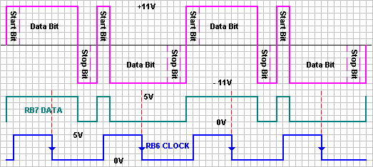
The chart below shows the wave forms generated by the circuit. The colours correspond to the circuit paths shown above.

You can see by the data here that as the RB6 clock pin is brought low, the data is already valid on the RB7 data pin. The data that would be clocked in from this chart is 1010.
To get these wave forms, the serial port is set to 1200 baud, 7 data bits, no parity, and 1 stop bit. The data above will be generated if these characters are sent...
#0 - NULL
#127 - DEL
#0 - NULL
#127 - DEL
Data Bit = 1
Data Bit = 0
Data Bit = 1
Data Bit = 0
These following character strings will program this instruction into the PIC at the current ROM address. All of the data is sent to the PIC with the LSB first. You will notice that we need to send one ASCII character for each data bit.
3014
MOVLW 14h
First we send the Load Data Command - 2h. This data is sent as 6 bits of information - 000010.
#127, #0, #127, #127, #127, #127
Now we send the ROM data. This consists of a Logic 0 Start Bit, followed by 14 bits of data, then a Logic 0 Stop Bit.
| Start | 4 | 1 | 0 |
|
|
#127, #127, #127, #0, #127, #0, #127, #127, #127, #127, #127, #127, #127, #0, #0, #127
To get the PIC to program that location, we use the Begin Programming Command - 8h. This data is sent as 6 bits of information - 001000.
#127, #127, #127, #0, #127, #127
This will be a very tedious task if your program is fairly large. One way around this could be to write a program in BASIC that will do the hard work for you. That will involve getting the HEX data from a compiled file and then converting each 1 bit to ASCII #0 and each 0 bit to ASCII #127 for each of the words that need to be programmed. Combine each of the ASCII values into a 'string' and then send it to the serial port.
One thing I haven't mentioned yet is the Vpp or Programming voltage. This needs to be around 13 Volts and it can be simply connected to the MCLR pin with a small switch. If the programmed PIC is to be used as a programmer, then that voltage and a 5 Volt supply is probably already available.
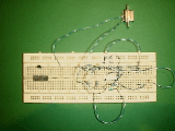
Here is a pretty messy bread boarded circuit, but it works ok.

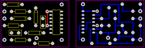
This is a PCB design for the programmer, if you would like to build one this way.

Click here to download the Programmer Software and a PDF file of the PCB and schematic. (130K)