Parts explanation (3)
of 4 Channel Adapter for the Oscilloscope
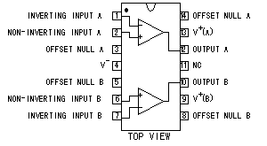 It houses two operational amplifiers in one package. Each operational amplifier can adjust an output offset. This time, it doesn't use. It houses two operational amplifiers in one package. Each operational amplifier can adjust an output offset. This time, it doesn't use.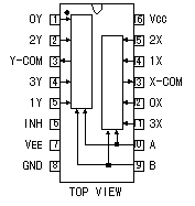 It switches four input signals by the condition of the control lines. The analog signal of ±5 V(peak) can be switched. Two sets of switches are housed in this IC. This time, it is using only one set. 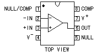 The operational amplifier except LM318 is OK.It is OK, LM6361N(luxurious), LM301, TL081, the others. It uses at mu factor 1 and not having been held in the extreme high efficiency about the frequency, too The operational amplifier except LM318 is OK.It is OK, LM6361N(luxurious), LM301, TL081, the others. It uses at mu factor 1 and not having been held in the extreme high efficiency about the frequency, too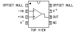 LM6361N is the operational amplifier IC with extremely good switching characteristic. As for usual IC(LM318), the slew rate is 50V/µS. However, 6361 is 300/µS. This shows that the IC can work at high speed. LM6361N is the operational amplifier IC with extremely good switching characteristic. As for usual IC(LM318), the slew rate is 50V/µS. However, 6361 is 300/µS. This shows that the IC can work at high speed.I used this IC for the wave form which is as sharp as possible to have oscillation. 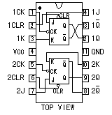 It is the IC to house two JK flip-flops in one package. It is the IC to house two JK flip-flops in one package.This time, it is using only one. I used HC type with little consumption electric power. 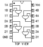 It is a 2 input NAND gate. Four 2 NAND gate circuits are housed in one package. 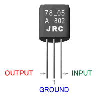 It is the IC to make the stable +5V voltage from +12 V. The output current is a maximum of 100 mA. Be careful because the lead line position is different from the regulator for the negative voltage (79L05). 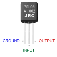 It is the IC to make the stable -5V voltage from -12 V. The output current is a maximum of 100 mA. Be careful because the lead line position is different from the regulator for the positive voltage (78L05). 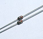 The Zener diode is used to limit the output voltage of the oscillator to about ±5 V. 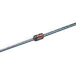 It is using to exclude the negative part with the output voltage of the oscillator.  It installs on the printed board to connect the wiring and to confirm the signal or the voltage. Because the about 40 pins connect, it cuts and uses the number of the necessity.  It uses to install the printed board to the case. It is OK rather than the one which is made from the metal, too. It doesn't care in the plastic one. 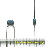 The digital circuit handles the square wave. As for the square wave, like the frequency, the high frequency component is contained. The voltage changes rapidly for the high frequency component to be contained. The high frequency component sometimes has an influence which is bad for the circuit to work. Because it is, the capacitor with the good high frequency characteristic can be put to the power circuit to lead the high frequency component to the ground (the 0-V potential). In case of the high frequency, the coil component of the copper wire becomes the resistance. So, the bypass capacitor is put in more than one of the wiring. The ceramic capacitor 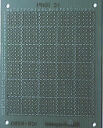 I used "30 X 25 halls" one as the printed board. Because it is sold from the various makers, you choose and use the one that the circuit to make suited. When the circuit is small, you cut in the suitable size and use. Universal PCB |