
 Bus Buffer ( 74HC125 ) Bus Buffer ( 74HC125 )
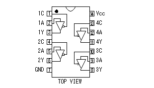
This is the bus buffer with 3-state outputs.
This IC is used to prevent a mutual influence on the side of the personal computer and the side of the CPLD device.
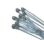
3 terminal regulator ( 78L05 )
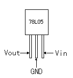
This regulator is used to make the stable power of +5 V.
The maximum output current is 100 mA.
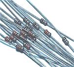
Diode ( 1S1588 )
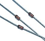
This diode is used for the countercurrent prevention of the power current.
IC socket
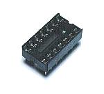
This socket is used to mount 74HC125.
When soldering IC directly to the printed board, it doesn't need.
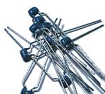
Resistor
Because the big crrent dosen't flow on this circuit, I am using 1/8W resistors.
Ceramic capacitor
These capacitors are used to bypass the high frequency noise of the JTAG signal.
Multilayer ceramic capacitor
These capacitors are used to bypass the high frequency noise.
Electrolytic capacitor
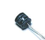
This capacitor is used to be stabilized of the input voltage and to bypass a low frequency noise.
Printed board
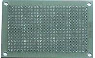
This is an universal printed board with 15 x 25 halls.
Wiring terminal
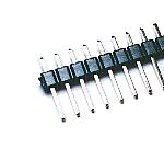
These terminala are used to connect the outside wires.
Stud
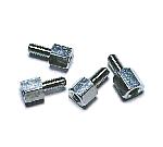
These parts are used to install a printed board in the case.
There are a lot of ground terminals of the socket. I grounded the wiring to the stud using the lug terminal.
Lug terminal
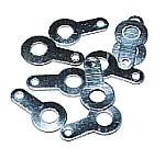
This terminal is used to connect the grounding wire of the PLCC socket.
|